SBAS659 November 2014 ADS58J89
PRODUCTION DATA.
- 1 Features
- 2 Applications
- 3 Description
- 4 Revision History
- 5 Pin Configuration and Functions
-
6 Specifications
- 6.1 Absolute Maximum Ratings
- 6.2 Handling Ratings
- 6.3 Recommended Operating Conditions
- 6.4 Thermal Information
- 6.5 Electrical Characteristics
- 6.6 Electrical Characteristics: 250 MSPS Output, 2x Decimation Filter
- 6.7 Electrical Characteristics: 500 MSPS Output
- 6.8 Electrical Characteristics: Sample Clock Timing Characteristics
- 6.9 Electrical Characteristics: Digital Outputs
- 6.10 Timing Requirements
- 6.11 Reset Timing
- 6.12 Typical Characteristics
-
7 Detailed Description
- 7.1 Overview
- 7.2 Functional Block Diagram
- 7.3
Feature Description
- 7.3.1 Decimation by 2 (250 MSPS Output)
- 7.3.2 Over-Range Indication
- 7.3.3 JESD204B Interface
- 7.3.4 SYSREF Clocking Schemes
- 7.3.5 Split-Mode Operation
- 7.3.6 Eye Diagram Information
- 7.3.7 Analog Inputs
- 7.3.8 Clock Inputs
- 7.3.9 Input Clock Divider
- 7.3.10 Power-Down Control
- 7.3.11 Device Configuration
- 7.3.12 JESD204B Interface Initialization Sequence
- 7.3.13 Device and Register Initialization
- 7.4 Device Functional Modes
- 7.5 Programming
- 7.6
Register Maps
- 7.6.1
Register Descriptions
- 7.6.1.1 Register Address 0
- 7.6.1.2 Register Address 1
- 7.6.1.3 Register Address 2
- 7.6.1.4 Register Address 3
- 7.6.1.5 Register Address 4
- 7.6.1.6 Register Address 5
- 7.6.1.7 Register Address 6
- 7.6.1.8 Register Address 7
- 7.6.1.9 Register Address 8
- 7.6.1.10 Register Address 12
- 7.6.1.11 Register Address 13
- 7.6.1.12 Register Address 14
- 7.6.1.13 Register Address 15
- 7.6.1.14 Register Address 16
- 7.6.1.15 Register Address 19
- 7.6.1.16 Register Address 22
- 7.6.1.17 Register Address 23
- 7.6.1.18 Register Address 26
- 7.6.1.19 Register Address 29
- 7.6.1.20 Register Address 30
- 7.6.1.21 Register Address 31
- 7.6.1.22 Register Address 32
- 7.6.1.23 Register Address 33
- 7.6.1.24 Address: 0x24, 0x25, 0x26, 0x27
- 7.6.1.25 Address: 0x28, 0x29, 0x2A, 0x2B
- 7.6.1.26 Register Address 44
- 7.6.1.27 Register Address 45
- 7.6.1.28 Register Address 46
- 7.6.1.29 Register Address 47
- 7.6.1.30 Address: 0x32, 0x33, 0x34, 0x35
- 7.6.1.31 Address: 0x36, 0x37, 0x38, 0x39
- 7.6.1.32 Register Address 58
- 7.6.1.33 Register Address 59
- 7.6.1.34 Register Address 60
- 7.6.1.35 Register Address 61
- 7.6.1.36 Register Address 99
- 7.6.1.37 Register Address 100
- 7.6.1.38 Register Address 103
- 7.6.1.39 Register Address 104
- 7.6.1.40 Register Address 107
- 7.6.1.41 Register Address 108
- 7.6.1.42 Register Address 111
- 7.6.1
Register Descriptions
- 8 Application and Implementation
- 9 Power Supply Recommendations
- 10Layout
- 11Device and Documentation Support
- 12Mechanical, Packaging, and Orderable Information
Package Options
Mechanical Data (Package|Pins)
- RGC|64
Thermal pad, mechanical data (Package|Pins)
- RGC|64
Orderable Information
1 Features
- 4-Ch, 14-Bit 500MSPS With Digital Signal Processing
- Power Amplifier Linearization (Feedback) Modes
- 14-Bits Every Other Sample at 250MSPS
- Programmable Resolution vs Duty Cycle
- Duty Cycle 3:2 (60% 11-Bit, 40% 9-Bit)
- Duty Cycle 2:3 (40% 12-Bit, 60% 9-Bit)
- Duty Cycle 1:3 (25% 14-Bit, 75% 9-Bit)
- Traffic Receiver Modes
- 14-Bit 250MSPS: Decimate by 2 Filter, High/Low Pass
- 9-Bit SNR-Boost Filter (150-MHz Max Bandwidth)
- 9-to-14-Bit TDD Burst (200-MHz Max Bandwidth)
- Flexible Input Clock Buffer With Divide by 1/2/4
- JESD204B Digital Interface up to 5.0Gbps
- 1 or 2 Lanes per Channel, With Subclass 1
- 64-Pin VQFN Package (9 × 9 mm)
2 Applications
- Multi-Carrier, Multi-Mode, Multi-Band Cellular Receivers
- TDD-LTE
- FDD-LTE
- CDMA, WCMDA, CMDA2k
- GSM
- RF and Microwave Backhaul
- Point-to-Point Backhaul
- Point-to-Multi-Point Backhaul
- Wireless Repeaters
- Distributed Antenna Systems (DAS)
- Broadband Wireless
3 Description
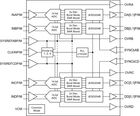
The ADS58J89 is a high-linearity, quad-channel, 14-bit, 250/500-MSPS IF (intermediate frequency) receiver. The four channels contain 500MSPS 14-bit ADCs followed by signal processing for wireless infrastructure systems. The channels can be configured in various modes depending on bandwidth, resolution and sample time requirements. The signal processing block contains selectable modes for decimation filters, SNR Boost filters, resolution versus time and time-division duplex (TDD) burst mode. Designed for high antenna count systems, the 4 channels provides high bandwidth and linearity to multi-channel receivers in a small footprint. The device can be dual function as traffic receiver and power amplifier linearization feedback path in TDD systems.
Key Specifications:
- Power Dissipation: 875 mW/ch
- Input Bandwidth (3dB): 900 MHz
- Aperture Jitter: 98 fs rms
- Channel Isolation: 85 dB
- Performance at ƒin = 170 MHz at 1.25 Vpp,
–1 dBFS- SNR: 65.8 dBFS
- SFDR: 85 dBc HD2,3; 95 dBFS non-HD2,3
Device Information(1)
| PART NUMBER | PACKAGE | MAX OUTPUT RATE |
|---|---|---|
| ADS58J89 | VQFN (64) | 500 MSPS |
- For all available packages, see the orderable addendum at the end of the data sheet.
Simplified Schematic
4 Revision History
| DATE | REVISION | NOTES |
|---|---|---|
| November 2014 | * | Initial release. |