SBAS659 November 2014 ADS58J89
PRODUCTION DATA.
- 1 Features
- 2 Applications
- 3 Description
- 4 Revision History
- 5 Pin Configuration and Functions
-
6 Specifications
- 6.1 Absolute Maximum Ratings
- 6.2 Handling Ratings
- 6.3 Recommended Operating Conditions
- 6.4 Thermal Information
- 6.5 Electrical Characteristics
- 6.6 Electrical Characteristics: 250 MSPS Output, 2x Decimation Filter
- 6.7 Electrical Characteristics: 500 MSPS Output
- 6.8 Electrical Characteristics: Sample Clock Timing Characteristics
- 6.9 Electrical Characteristics: Digital Outputs
- 6.10 Timing Requirements
- 6.11 Reset Timing
- 6.12 Typical Characteristics
-
7 Detailed Description
- 7.1 Overview
- 7.2 Functional Block Diagram
- 7.3
Feature Description
- 7.3.1 Decimation by 2 (250 MSPS Output)
- 7.3.2 Over-Range Indication
- 7.3.3 JESD204B Interface
- 7.3.4 SYSREF Clocking Schemes
- 7.3.5 Split-Mode Operation
- 7.3.6 Eye Diagram Information
- 7.3.7 Analog Inputs
- 7.3.8 Clock Inputs
- 7.3.9 Input Clock Divider
- 7.3.10 Power-Down Control
- 7.3.11 Device Configuration
- 7.3.12 JESD204B Interface Initialization Sequence
- 7.3.13 Device and Register Initialization
- 7.4 Device Functional Modes
- 7.5 Programming
- 7.6
Register Maps
- 7.6.1
Register Descriptions
- 7.6.1.1 Register Address 0
- 7.6.1.2 Register Address 1
- 7.6.1.3 Register Address 2
- 7.6.1.4 Register Address 3
- 7.6.1.5 Register Address 4
- 7.6.1.6 Register Address 5
- 7.6.1.7 Register Address 6
- 7.6.1.8 Register Address 7
- 7.6.1.9 Register Address 8
- 7.6.1.10 Register Address 12
- 7.6.1.11 Register Address 13
- 7.6.1.12 Register Address 14
- 7.6.1.13 Register Address 15
- 7.6.1.14 Register Address 16
- 7.6.1.15 Register Address 19
- 7.6.1.16 Register Address 22
- 7.6.1.17 Register Address 23
- 7.6.1.18 Register Address 26
- 7.6.1.19 Register Address 29
- 7.6.1.20 Register Address 30
- 7.6.1.21 Register Address 31
- 7.6.1.22 Register Address 32
- 7.6.1.23 Register Address 33
- 7.6.1.24 Address: 0x24, 0x25, 0x26, 0x27
- 7.6.1.25 Address: 0x28, 0x29, 0x2A, 0x2B
- 7.6.1.26 Register Address 44
- 7.6.1.27 Register Address 45
- 7.6.1.28 Register Address 46
- 7.6.1.29 Register Address 47
- 7.6.1.30 Address: 0x32, 0x33, 0x34, 0x35
- 7.6.1.31 Address: 0x36, 0x37, 0x38, 0x39
- 7.6.1.32 Register Address 58
- 7.6.1.33 Register Address 59
- 7.6.1.34 Register Address 60
- 7.6.1.35 Register Address 61
- 7.6.1.36 Register Address 99
- 7.6.1.37 Register Address 100
- 7.6.1.38 Register Address 103
- 7.6.1.39 Register Address 104
- 7.6.1.40 Register Address 107
- 7.6.1.41 Register Address 108
- 7.6.1.42 Register Address 111
- 7.6.1
Register Descriptions
- 8 Application and Implementation
- 9 Power Supply Recommendations
- 10Layout
- 11Device and Documentation Support
- 12Mechanical, Packaging, and Orderable Information
Package Options
Mechanical Data (Package|Pins)
- RGC|64
Thermal pad, mechanical data (Package|Pins)
- RGC|64
Orderable Information
6 Specifications
6.1 Absolute Maximum Ratings
over operating free-air temperature (unless otherwise noted)(1)| MIN | MAX | UNIT | ||
|---|---|---|---|---|
| Supply voltage | AVDD33 | –0.3 | 3.6 | V |
| AVDD18 | –0.3 | 2.1 | ||
| AVDDC | –0.3 | 2.1 | ||
| DVDD | –0.3 | 2.1 | ||
| IOVDD | –0.3 | 2.1 | ||
| PLLVDD | –0.3 | 2.1 | ||
| Voltage between AGND and DGND | –0.3 | 0.3 | V | |
| Voltage applied to input pins | INAP, INBP, INCP, INDP, INAM, INBM, INCM, INDM | –0.3 | 3 | V |
| CLKINP, CLKINM | –0.3 | AVDD18 + 0.3 V | ||
| SYNCbABP, SYNCbABM, SYNCbCDP, SYNCbCDM | –0.3 | AVDD18 + 0.3 V | ||
| SYSREFABP, SYSREFABM, SYSREFCDP, SYSREFCDM | –0.3 | AVDD18 + 0.3 V | ||
| SCLK, SDENb, SDATA, SRESETb, ENABLE | –0.3 | DVDD + 0.5 V | ||
| TA | Operating free-air temperature | –40 | 85 | ºC |
| TJ | Operating junction temperature(2) | 125 | ºC | |
(1) Stresses beyond those listed as absolute maximum ratings may cause permanent damage to the device. These are stress ratings only, and functional operation of the device at these or any other conditions beyond those indicated as recommended operating conditions is not implied. Exposure to absolute-maximum-rated conditions for extended periods may affect device reliability.
(2) Prolonged use at this junction temperature may increase the device failure-in-time (FIT) rate.
6.2 Handling Ratings
| MIN | MAX | UNIT | |||
|---|---|---|---|---|---|
| Tstg | Storage temperature | –65 | 150 | °C | |
| VESD | Electrostatic discharge | Human body model (HBM), per ANSI/ESDA/JEDEC JS-001, all pins(1) | –2 | 2 | kV |
(1) JEDEC document JEP155 states that 500-V HBM allows safe manufacturing with a standard ESD control process.
6.3 Recommended Operating Conditions
over operating free-air temperature range (unless otherwise noted)| MIN | NOM | MAX | UNIT | |||
|---|---|---|---|---|---|---|
| ADC clock frequency | 250 | 500 | MSPS | |||
| Resolution | 14 | 14 | bits | |||
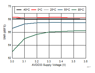
| Supply | AVDD33 | 3.15 | 3.3 | 3.45 | V | |
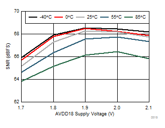
| AVDD18 | 1.8 | 1.9 | 2.0 | |||
| AVDDC | 1.7 | 1.8 | 1.9 | |||
| DVDD | 1.7 | 1.8 | 1.9 | |||
| IOVDD | 1.7 | 1.8 | 1.9 | |||
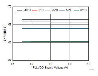
| PLLVDD | 1.7 | 1.8 | 1.9 | |||
| TA | Operating free-air temperature | –40 | 85 | °C | ||
| TJ | Operating junction temperature | 125 | °C | |||
6.4 Thermal Information
| Thermal Metric(1) | RGC (64 PINS) | UNIT | |
|---|---|---|---|
| RΘJA | Junction-to-ambient thermal resistance | 23.5 | °C/W |
| RΘJC(top) | Junction-to-case, top | 7.0 | |
| RΘJB | Junction-to-board thermal resistance | 2.6 | |
| φJT | Junction-to-top of package | 0.1 | |
| φJB | Junction-to-board characterization parameter | 2.6 | |
| RΘJC(bot) | Junction-to-case, bottom | 0.3 | |
(1) For more information about traditional and new thermal metrics, see the IC Package Thermal Metrics application report, SPRA953.
6.5 Electrical Characteristics
Typical values at TA = 25°C, full temperature range is TMIN = –40°C to TMAX = 85°C, ADC sampling rate = 500 MSPS, 50% clock duty cycle, AVDD33 = 3.3 V; AVDD18 = 1.9 V; AVDDC, DVDD, IOVDD, PLLVDD = 1.8 V, –1-dBFS differential input, unless otherwise noted.| PARAMETER | TEST CONDITIONS | MIN | TYP | MAX | UNIT | ||
|---|---|---|---|---|---|---|---|
| POWER SUPPLY | |||||||
| IAVDD33 | 3.3-V analog supply current | 500 | mA | ||||
| IAVDD18 | 1.9-V analog supply current | 320 | mA | ||||
| IAVDDC | 1.8-V clock supply current | 18 | mA | ||||
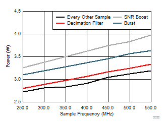
| IDVDD | 1.8-V digital supply current | 4-channel SNR boost | 472 | mA | |||
| 4-channel decimation filter | 323 | ||||||
| 4-channel burst mode | 324 | ||||||
| 2-channel burst mode, 2-channel SNR boost | 398 | ||||||
| 2-channel decimation filter, 2-channel burst mode | 324 | ||||||
| 2-channel decimation filter, 2-channel, discard every other sample | 289 | ||||||
| IIOVDD | I/O voltage supply current | 2 lanes per ADC | 373 | mA | |||
| 1 lane per ADC | 185 | ||||||
| IPLLVDD | PLL voltage supply current | 42 | mA | ||||
| Pdis | Total power dissipation | 4-channel SNR boost | 3.94 | W | |||
| 4-channel Burst mode | 3.67 | ||||||
| 4-channel decimation filter | 3.34 | ||||||
| 4-channel decimation filter, 1 lane per ADC | 3.27 | 3.5 | |||||
| 2-channel SNR Boost, 2-channel burst mode | 3.81 | ||||||
| 2-channel decimation filter, 2-channel burst mode | 3.51 | ||||||
| 2-channel decimation filter, 2-channel, discard every other sample | 3.28 | ||||||
| Deep sleep mode power | 791 | mW | |||||
| Wake-up time from deep sleep mode | SNR > 60 dB | 1.4 | ms | ||||
| Light sleep mode power | 1.68 | W | |||||
| Wake-up time from light sleep mode | SNR > 60 dB | 8 | µs | ||||
| ANALOG INPUTS | |||||||
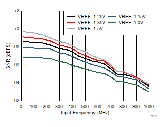
| Differential input full-scale | 1.0 | 1.25 | 1.5 | Vpp | |||
| Input common mode voltage | Vcm ± 50 mV | V | |||||
| Input resistance | Differential at DC | 1 | kΩ | ||||
| Input capacitance | Each input to GND | 2.75 | pF | ||||
| VCM | Common mode voltage output | 2.18 | V | ||||
| Analog input bandwidth (–3 dB) | 900 | MHz | |||||
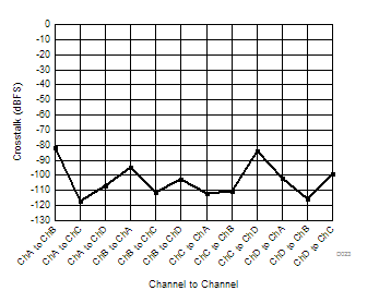
| CHANNEL-TO-CHANNEL ISOLATION | |||||||
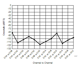
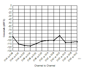
| Crosstalk(1) | Near channel | ƒIN = 170 MHz | 85 | dB | |||
| Far channel | ƒIN = 170 MHz | 95 | |||||
| CLOCK INPUT | |||||||
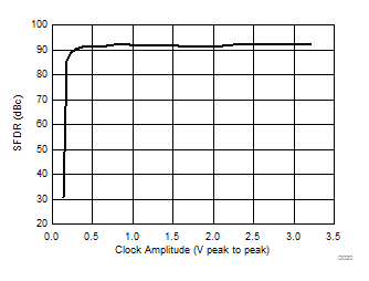
| Input clock frequency | 250 | 2000(2) | MHz | ||||
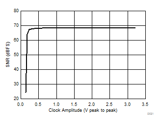
| Input clock amplitude | 0.4 | 1.5 | Vpp | ||||
| Input clock duty cycle | 45% | 50% | 55% | ||||
| Internal clock biasing | 0.9 | V | |||||
(1) Crosstalk is measured with a –1-dBFS input signal on aggressor channel and no input on victim channel.
(2) CLK / 4 mode
6.6 Electrical Characteristics: 250 MSPS Output, 2x Decimation Filter
Typical values at TA = 25°C, full temperature range is TMIN = –40°C to TMAX = 85°C, ADC sampling rate = 500 MSPS, 50% clock duty cycle, AVDD33 = 3.3 V; AVDD18 = 1.9 V; AVDDC, DVDD, IOVDD, PLLVDD = 1.8 V, –1-dBFS differential input, unless otherwise noted.| PARAMETER | TEST CONDITIONS | MIN | TYP | MAX | UNIT | ||
|---|---|---|---|---|---|---|---|
| SNR | Signal-to-noise ratio | ƒIN = 10 MHz | 68.3 | dBFS | |||
| ƒIN = 100 MHz | 68.2 | ||||||
| ƒIN = 170 MHz | 65 | 68.2 | |||||
| ƒIN = 310 MHz | 67.6 | ||||||
| ƒIN = 450 MHz | 66.8 | ||||||
| HD2 | Second harmonic distortion | ƒIN = 10 MHz | 85 | dBc | |||
| ƒIN = 100 MHz | 85 | ||||||
| ƒIN = 170 MHz | 75 | 85 | |||||
| ƒIN = 310 MHz | 85 | ||||||
| ƒIN = 450 MHz | 75 | ||||||
| HD3 | Third harmonic distortion | ƒIN = 10 MHz | 85 | dBc | |||
| ƒIN = 100 MHz | 85 | ||||||
| ƒIN = 170 MHz | 75 | 85 | |||||
| ƒIN = 310 MHz | 85 | ||||||
| ƒIN = 450 MHz | 85 | ||||||
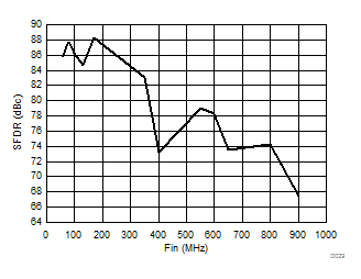
| SFDR (Non-HD2, Non-HD3) |
Spur free dynamic range (excluding HD2 and HD3) |
ƒIN = 10 MHz | 95 | dBc | |||
| ƒIN = 100 MHz | 95 | ||||||
| ƒIN = 170 MHz | 75 | 95 | |||||
| ƒIN = 310 MHz | 90 | ||||||
| ƒIN = 450 MHz | 85 | ||||||
| IMD3 | 2F1-F2, 2F2-F1, Ain = –7 dBFS | FIN = 169 and 171 MHz | 93 | dBFS | |||
6.7 Electrical Characteristics: 500 MSPS Output
Typical values at TA = 25°C, full temperature range is TMIN = –40°C to TMAX = 85°C, ADC sampling rate = 500 MSPS, 50% clock duty cycle, AVDD33 = 3.3 V; AVDD18 = 1.9 V; AVDDC, DVDD, IOVDD, PLLVDD = 1.8 V, –1-dBFS differential input, unless otherwise noted.| PARAMETER | TEST CONDITIONS | MIN | TYP | MAX | UNIT | ||
|---|---|---|---|---|---|---|---|
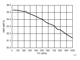
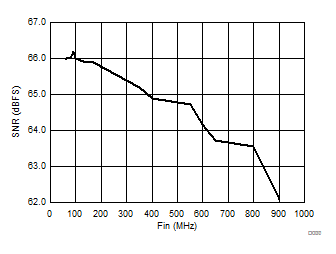
| SNR | Signal-to-Noise Ratio | SNR Boost (150-MHz bandwidth) | ƒIN = 100 MHz | 65.7 | dBFS | ||
| ƒIN = 170 MHz | 65.7 | ||||||
| ƒIN = 350 MHz | 65 | ||||||
| Burst Mode (14 bit) | ƒIN = 10 MHz | 65.3 | dBFS | ||||
| ƒIN = 100 MHz | 65.2 | ||||||
| ƒIN = 170 MHz | 65.1 | ||||||
| ƒIN = 370 MHz | 64.7 | ||||||
| ƒIN = 450 MHz | 64.6 | ||||||
| HD2 | Second Harmonic Distortion | ƒIN = 10 MHz | 85 | dBc | |||
| ƒIN = 100 MHz | 85 | ||||||
| ƒIN = 170 MHz | 85 | ||||||
| ƒIN = 370 MHz | 75 | ||||||
| ƒIN = 450 MHz | 75 | ||||||
| HD3 | Third Harmonic Distortion | ƒIN = 10 MHz | 85 | dBc | |||
| ƒIN = 100 MHz | 85 | ||||||
| ƒIN = 170 MHz | 85 | ||||||
| ƒIN = 370 MHz | 78.3 | ||||||
| ƒIN = 450 MHz | 85 | ||||||
| SFDR (Non-HD2, Non-HD3) |
Spur Free Dynamic Range (excluding HD2 and HD3) |
ƒIN = 10 MHz | 85 | dBFS | |||
| ƒIN = 100 MHz | 85 | ||||||
| ƒIN = 170 MHz | 85 | ||||||
| ƒIN = 370 MHz | 83 | ||||||
| ƒIN = 450 MHz | 83 | ||||||
| IMD3 | 2F1-F2, 2F2-F1, Ain = –7 dBFS | FIN = 169 and 171 MHz | 87 | dBFS | |||
6.8 Electrical Characteristics: Sample Clock Timing Characteristics
Typical values at TA = 25°C, full temperature range is TMIN = –40°C to TMAX = 85°C, ADC sampling rate = 500 MSPS, 50% clock duty cycle, AVDD33 = 3.3 V; AVDD18 = 1.9 V; AVDDC, DVDD, IOVDD, PLLVDD = 1.8 V, –1 dBFS differential input, unless otherwise noted.| PARAMETER | MIN | TYP | MAX | UNIT | |
|---|---|---|---|---|---|
| Aperture jitter, RMS | 98 | fs rms | |||
| Data latency | 38 | Sample clock cycles | |||
| Fast over-range (OVR) latency | 6 | ||||
| tPDI | Clock aperture delay | 1.1 | ns | ||
6.9 Electrical Characteristics: Digital Outputs
The DC specifications refer to the condition where the digital outputs are not switching, but are permanently at a valid logic level 0 or 1. AVDD33 = 3.3 V; AVDD18 = 1.9 V; AVDDC, DVDD, IOVDD, PLLVDD = 1.8 V.| PARAMETER | MIN | TYP | MAX | UNIT | |
|---|---|---|---|---|---|
| DIGITAL OUTPUTS: JESD204B INTERFACE (DA[0,1], DB[0,1], DC[0,1], DD[0,1]) |
|||||
| Output differential voltage, |VOD| | 450 | 577 | 750 | mV | |
| Transmitter short circuit current | Transmitter terminals shorted to any voltage between –0.25 and 1.45 V | 45 | mA | ||
| Single ended output impedance | 50 | Ω | |||
| Output capacitance | Output capacitance inside the device, from either output to ground | 2 | pF | ||
| Unit interval, UI | 5.0 Gbps | 200 | ps | ||
| Rise and fall times | 110 | ps | |||
| Output jitter | 57 | ps | |||
| Serial output data rate | 5.0 | Gbps | |||
6.10 Timing Requirements
| MIN | TYP | MAX | UNIT | ||
|---|---|---|---|---|---|
| DIGITAL INPUTS: SRESETb, SCLK, SDENb, SDATA, ENABLE, OVRA, OVRC, SYSREFCDP, SYSREFCDM |
|||||
| High-level input voltage | All digital inputs support 1.8-V and 3.3-V logic levels | 1.2 | V | ||
| Low-level input voltage | 0.4 | V | |||
| High-level input current | 50 | µA | |||
| Low-level input current | –50 | µA | |||
| Input capacitance | 4 | pF | |||
| DIGITAL OUTPUTS: SDOUT, OVRA, OVRB, OVRC, OVRD |
|||||
| High-level output voltage | ILoad = –100 µA | DVDD – 0.2 | DVDD | V | |
| Low-level output voltage | 0.2 | V | |||
| DIGITAL INPUTS: SYNCbABP/M, SYNCbCDP/M, SYSREFABP/M, SYSREFCDP/M |
|||||
| Input voltage VID | 250 | 350 | 450 | mV | |
| Input common mode voltage VCM | 0.4 | 0.9 | 1.4 | V | |
| tS_SYSREFxx | Referenced to rising edge of input clock | 100 | ps | ||
| tH_SYSREFxx | Referenced to rising edge of input clock | 100 | ps | ||
6.11 Reset Timing
| PARAMETER | TEST CONDITIONS | MIN | TYP | MAX | UNIT | |
|---|---|---|---|---|---|---|
| t1 | Power-on delay | Delay from power up to active-low RESET pulse | 3 | ms | ||
| t2 | Reset pulse duration | Active-low RESET pulse duration | 20 | ns | ||
| t3 | Register write delay | Delay from RESET disable to SDENb active | 100 | ns | ||
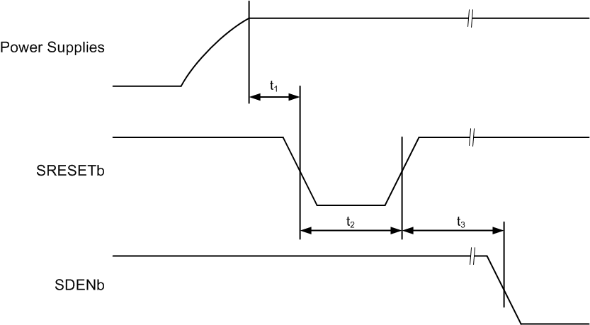 Figure 1. Reset Timing Diagram
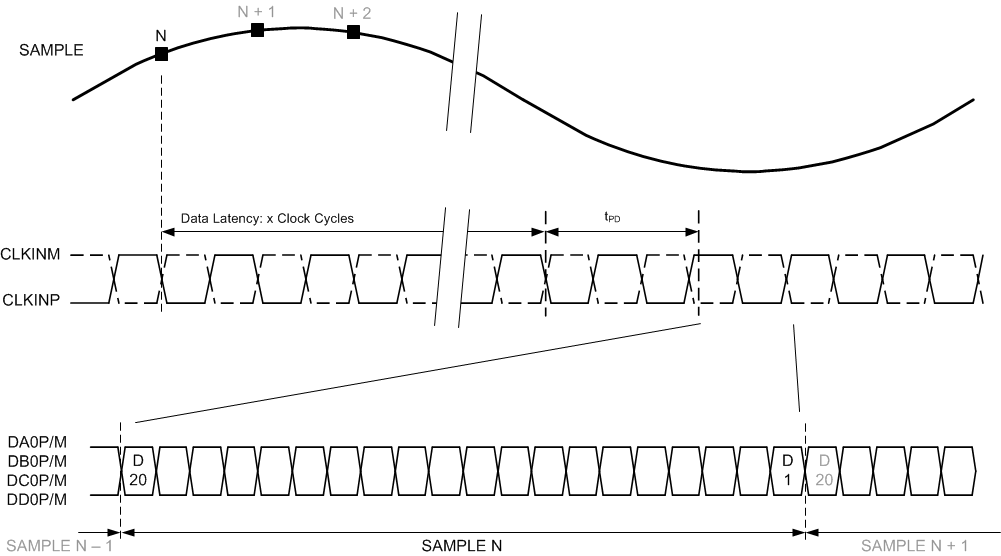
A. tPD is the propagation delay from sample clock input edge to serial data output transition
Figure 2. Timing Diagram: 250 MSPS Output Data Rate
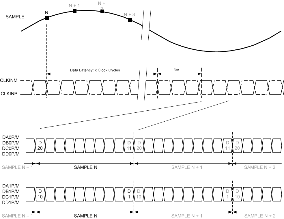
A. tPD is the propagation delay from sample clock input edge to serial data output transition
Figure 3. Timing Diagram: 500 MSPS Output Data Rate
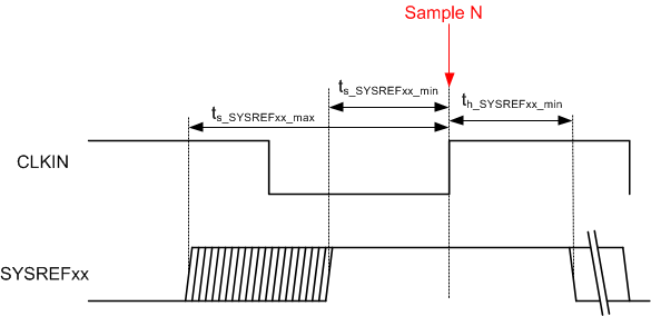 Figure 4. Timing Using SYSREF (Subclass 1)
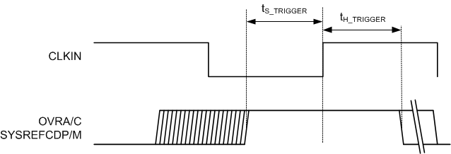
A. Trigger is allowed to be asynchronous to the sample clock. If the trigger input does not meet setup and hold timing around one clock cycle, then the trigger will be caught on the next cycle.
Figure 5. Timing for External Manual Trigger Input
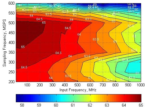
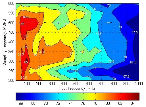
6.12 Typical Characteristics
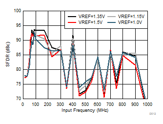
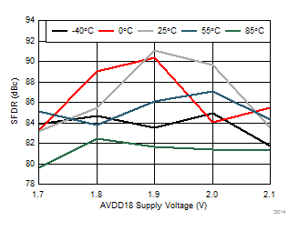
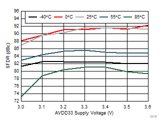
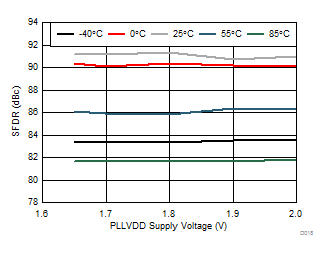
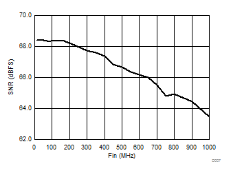
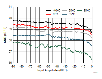
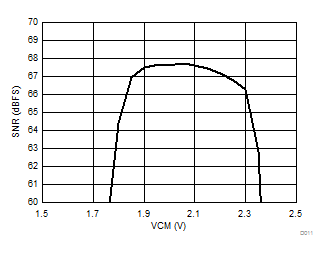
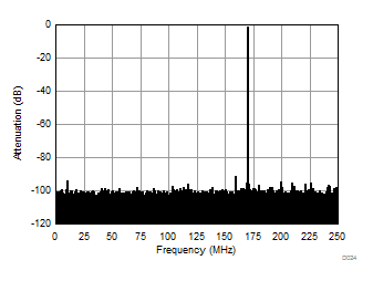
Typical values at TA = 25°C, full temperature range is TMIN = –40°C to TMAX = 85°C, Device clock frequency = 500 MHz, Output sample data rate = 5Gbps, 50% Device clock duty cycle, AVDD33 = 3.3 V, AVDD18 = 1.9 V, AVDDC = 1.8 V, IOVDD = 1.8 V, PLLVDD = 1.8 V, DVDD = 1.8 V, –1 dBFS differential input, unless otherwise noted, FFT sample size = 32768.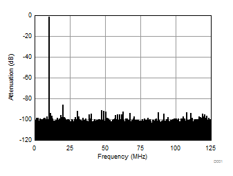
| Fin = 10 MHz | 1-lane 2x decimation | Ain = –1 dBFS |
| SNR = 65.29 dBFS | SFDR = 84.72 dBc |
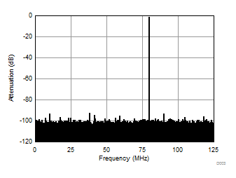
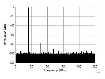
| Fin = 170 MHz | 1-lane 2x decimation | Ain = –1 dBFS |
| SNR = 65.34 dBFS | SFDR = 91.62 dBc |
| 1-lane 2x decimation | Ain = –1 dBFS |
| 1-lane 2x decimation | Fin = –170 MHz |
| 1-lane 2x decimation | Fin = –170 MHz |
| 1-lane 2x decimation | Ain = –1 dBFS |
| 1-lane 2x decimation | Ain = –1 dBFS | Fin = 170 MHz |
| 1-lane 2x decimation | Ain = –1 dBFS | Fin = 170 MHz |
| 1-lane 2x decimation | Ain = –1 dBFS | Fin = 170 MHz |
| 1-lane 2x decimation | Ain = –1 dBFS | Fin = 170 MHz |
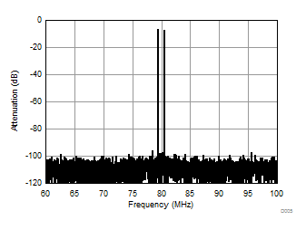
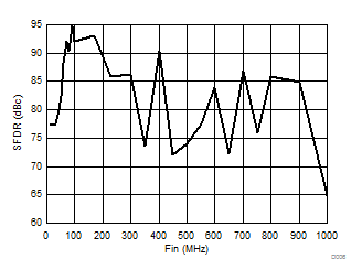
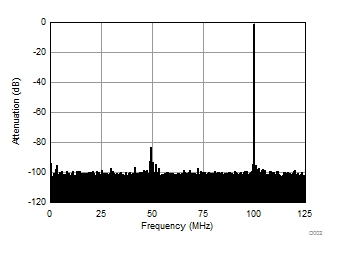
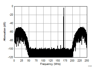
| Fin = 170 MHz | 1-MHz spacing | 1-lane 2x decimation |
| Ain = –7 dBFS | 60 to 100 MHz shown |
| 1-lane 2x decimation | Ain = –1 dBFS | Fin = 170 MHz |
| 2-lane burst mode | Ain = –1 dBFS |
| 2-lane burst mode | Ain = –1 dBFS | Fin = 170 MHz |
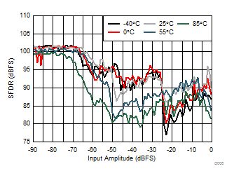
| 2-lane SNR boost mode | Ain = –1 dBFS | |
| Blackman-Harris filter |
| 2-lane SNR boost mode | Ain = –1 dBFS | Fin = 170 MHz | ||
| Fin = 100 MHz | 1-lane 2x decimation | Ain = –1 dBFS |
| SNR = 65.40 dBFS | SFDR = 82.50 dBc |
| Fin = 230 MHz | 1-lane 2x decimation | Ain = –1 dBFS |
| SNR = 65.16 dBFS | SFDR = 76.83 dBc |
| 1-lane 2x decimation | Ain = –1 dBFS |
| 1-lane 2x decimation | Fin = –170 MHz |
| 1-lane 2x decimation | Fin = –170 MHz |
| 1-lane 2x decimation | Ain = –1 dBFS |
| 1-lane 2x decimation | Ain = –1 dBFS | Fin = 170 MHz |
| 1-lane 2x decimation | Ain = –1 dBFS | Fin = 170 MHz |
| 1-lane 2x decimation | Ain = –1 dBFS | Fin = 170 MHz |
| 1-lane 2x decimation | Ain = –1 dBFS | Fin = 170 MHz |
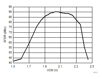
| AVDD18 = 1.9 V | AVDD33 = 3.3 V | Other supplies = 1.8 V |
| Ain = –1 dBFS | Fin = 170 MHz |
| 2-lane burst mode | Ain = –1 dBFS | Fin = 170 MHz |
| SNR = 65.26 dBFS | SFDR = 90.42 dBc |
| 2-lane burst mode | Ain = –1 dBFS |
| 2-lane SNR boost mode | Ain = –1 dBFS | Fin = 170 MHz |
| Blackman-Harris filter |
| 2-lane SNR boost mode | Ain = –1 dBFS | |
| Blackman-Harris filter |