SBAS659 November 2014 ADS58J89
PRODUCTION DATA.
- 1 Features
- 2 Applications
- 3 Description
- 4 Revision History
- 5 Pin Configuration and Functions
-
6 Specifications
- 6.1 Absolute Maximum Ratings
- 6.2 Handling Ratings
- 6.3 Recommended Operating Conditions
- 6.4 Thermal Information
- 6.5 Electrical Characteristics
- 6.6 Electrical Characteristics: 250 MSPS Output, 2x Decimation Filter
- 6.7 Electrical Characteristics: 500 MSPS Output
- 6.8 Electrical Characteristics: Sample Clock Timing Characteristics
- 6.9 Electrical Characteristics: Digital Outputs
- 6.10 Timing Requirements
- 6.11 Reset Timing
- 6.12 Typical Characteristics
-
7 Detailed Description
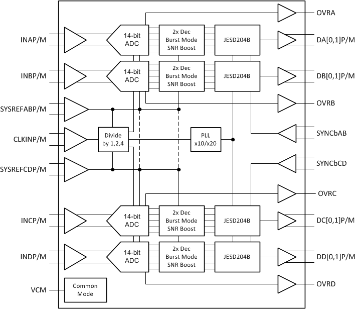
- 7.1 Overview
- 7.2 Functional Block Diagram
- 7.3
Feature Description
- 7.3.1 Decimation by 2 (250 MSPS Output)
- 7.3.2 Over-Range Indication
- 7.3.3 JESD204B Interface
- 7.3.4 SYSREF Clocking Schemes
- 7.3.5 Split-Mode Operation
- 7.3.6 Eye Diagram Information
- 7.3.7 Analog Inputs
- 7.3.8 Clock Inputs
- 7.3.9 Input Clock Divider
- 7.3.10 Power-Down Control
- 7.3.11 Device Configuration
- 7.3.12 JESD204B Interface Initialization Sequence
- 7.3.13 Device and Register Initialization
- 7.4 Device Functional Modes
- 7.5 Programming
- 7.6
Register Maps
- 7.6.1
Register Descriptions
- 7.6.1.1 Register Address 0
- 7.6.1.2 Register Address 1
- 7.6.1.3 Register Address 2
- 7.6.1.4 Register Address 3
- 7.6.1.5 Register Address 4
- 7.6.1.6 Register Address 5
- 7.6.1.7 Register Address 6
- 7.6.1.8 Register Address 7
- 7.6.1.9 Register Address 8
- 7.6.1.10 Register Address 12
- 7.6.1.11 Register Address 13
- 7.6.1.12 Register Address 14
- 7.6.1.13 Register Address 15
- 7.6.1.14 Register Address 16
- 7.6.1.15 Register Address 19
- 7.6.1.16 Register Address 22
- 7.6.1.17 Register Address 23
- 7.6.1.18 Register Address 26
- 7.6.1.19 Register Address 29
- 7.6.1.20 Register Address 30
- 7.6.1.21 Register Address 31
- 7.6.1.22 Register Address 32
- 7.6.1.23 Register Address 33
- 7.6.1.24 Address: 0x24, 0x25, 0x26, 0x27
- 7.6.1.25 Address: 0x28, 0x29, 0x2A, 0x2B
- 7.6.1.26 Register Address 44
- 7.6.1.27 Register Address 45
- 7.6.1.28 Register Address 46
- 7.6.1.29 Register Address 47
- 7.6.1.30 Address: 0x32, 0x33, 0x34, 0x35
- 7.6.1.31 Address: 0x36, 0x37, 0x38, 0x39
- 7.6.1.32 Register Address 58
- 7.6.1.33 Register Address 59
- 7.6.1.34 Register Address 60
- 7.6.1.35 Register Address 61
- 7.6.1.36 Register Address 99
- 7.6.1.37 Register Address 100
- 7.6.1.38 Register Address 103
- 7.6.1.39 Register Address 104
- 7.6.1.40 Register Address 107
- 7.6.1.41 Register Address 108
- 7.6.1.42 Register Address 111
- 7.6.1
Register Descriptions
- 8 Application and Implementation
- 9 Power Supply Recommendations
- 10Layout
- 11Device and Documentation Support
- 12Mechanical, Packaging, and Orderable Information
Package Options
Mechanical Data (Package|Pins)
- RGC|64
Thermal pad, mechanical data (Package|Pins)
- RGC|64
Orderable Information
7 Detailed Description
7.1 Overview
The ADS58J89 is a pin-to-pin compatible, very-low power, wide bandwidth 14-bit 250 or 500 MSPS quad channel receiver and feedback IC. It supports the JESD204B serial interface with data rates up to 5.0 Gbps supporting 1 or 2 lanes per channel. The buffered analog input provides uniform input impedance across a wide frequency range while minimizing sample-and-hold glitch energy. A sampling clock divider allows more flexibility for system clock architecture design. The ADS58J89 provides excellent SFDR over a large input frequency range with very-low power consumption.
7.2 Functional Block Diagram
7.3 Feature Description
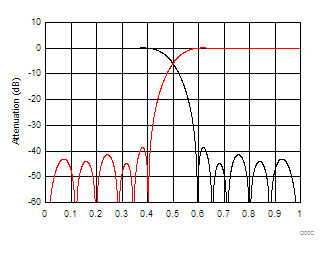
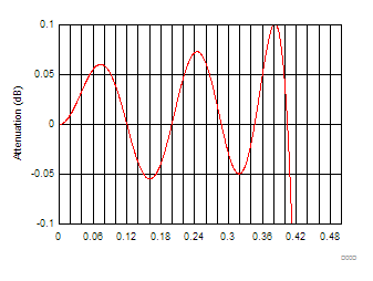
7.3.1 Decimation by 2 (250 MSPS Output)
Each channel has a digital filter in the data path as shown in Figure 39. The filter can be programmed as a low-pass or high-pass filter and the normalized frequency response of both filters is shown in Figure 40.
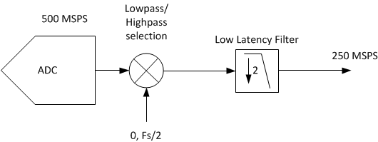 Figure 39. 2x Decimation Filter
The decimation filter response has a 0.1-dB pass band ripple with approximately 41% pass-band bandwidth. The stop-band attenuation is approximately 40 dB.
7.3.2 Over-Range Indication
The ADS58J89 provides a fast over-range indication on the OVRA, OVRB, OVRC, and OVRD pins. The fast OVR is triggered if the input voltage exceeds the programmable over-range threshold and is output after just 6 clock cycles, enabling a quicker reaction to an over-range event. The OVR threshold can be configured using SPI register writes.
The input voltage level at which the overload is detected is referred to as the threshold and is programmable using the over-range threshold bits.
The threshold at which fast OVR is triggered is (full-scale × [the decimal value of the FAST OVR THRESH bits] / 8). After reset, the default value of the over-range threshold is set to 7 (decimal), which corresponds to a threshold of 1.12 dB below full scale (20 × log(7/8)).
Table 1. Fast Over Range Threshold Settings
| OVR Setting (decimal) | OVR Threshold (dBFS) |
|---|---|
| 1 | –18.1 |
| 2 | –12.0 |
| 3 | –8.5 |
| 4 | –6.0 |
| 5 | –4.1 |
| 6 | –2.5 |
| 7 (default) | –1.1 |
Because the fast over-range indicator is single-ended LVCMOS logic, the ADS58J89 device can be configured through the SPI register write to keep the over-range indicator asserted high for an extra one, two, or four clock cycles. This longer assertion of the signal ensures the processor can capture the over-range event.
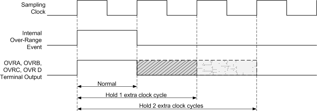 Figure 42. Fast Over Range Output Timing
The ADS58J89 device also provides the fast over-range indication bit in the JESD204B output data stream.
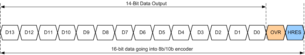 Figure 43. Sample Data and Status Bit Format
7.3.3 JESD204B Interface
The ADS58J89 supports device subclass 1 with a maximum output data rate of 5.0 Gbps for each serial transmitter. It allows independent JESD204B format configuration for channel A and B and channel C and D.
An external SYSREF signal is used to align all internal clock phases and the local multi-frame clock to a specific sampling clock edge. This allows synchronization of multiple devices in a system and minimizes timing and alignment uncertainty. SYNCbAB input is used to control all the JESD204B SerDes blocks for channel A and B while SYNCbCD is used to control channel C and D. If the same LMFS configuration is used for all four channels, the SYNCbAB and SYNCbCD signals can be tied together externally and driven from the same source.
Depending on the channel output data rate, the JESD204B output interface can be operated with either 1 or 2 lanes per single channel. The JESD204B setup and configuration of the frame assembly parameters are controlled via SPI interface.
The JESD204B transmitter block consists of the transport layer, the data scrambler and the link layer. The transport layer maps the channel output data into the selected JESD204B frame data format and manages if the channel output data or test patterns are being transmitted. The link layer performs the 8b/10b data encoding as well as the synchronization and initial lane alignment using the SYNCb input signal. Optionally, data from the transport layer can be scrambled.
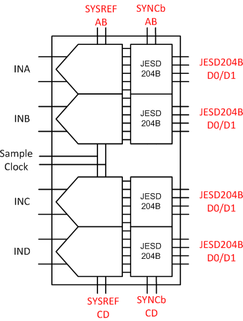 Figure 44. JESD204B Lane Assignment
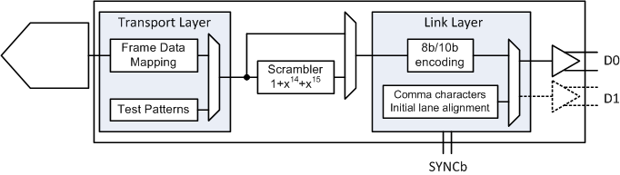 Figure 45. JESD204B Block
7.3.3.1 JESD204B Initial Lane Alignment (ILA)
The ILA process is started by the receiving device by deasserting the SYNCb signal. Upon detecting a logic low on the SYNCbAB input pins, the ADS58J89 device starts transmitting comma (K28.5) characters on channels A and B to establish code group synchronization. Upon detecting a logic high on the SYNCbCD input pins, the ADS58J89 device starts transmitting comma (K28.5) characters on channels C and D to establish code group synchronization.
After synchronization is completed, the receiving device asserts the SYNCb signal and the ADS58J89 starts the ILA sequence with the next local multi-frame clock boundary. The ADS58J89 device transmits 4 multi-frames each containing K frames (K is SPI programmable). Each of the multi-frames contains the frame start and end symbols and the second multi-frame also contains the JESD204 link configuration data.
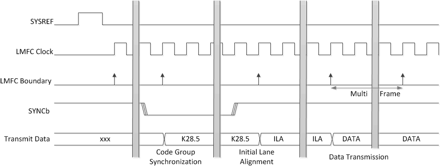 Figure 46. Initial Lane Assignment Format
7.3.3.2 JESD204B Test Patterns
There are three different test patterns available in the transport layer of the JESD204B interface. The ADS58J89 supports a RAMP, 1555/2AAA and different PRBS patterns. They can be enabled through SPI register write and are located in address 0x1D and 0x32/33.
7.3.3.3 JESD204B Frame Assembly
The JESD204B standard defines the following parameters:
- L = number of lanes per link
- M = number of converters for device
- F = number of octets per frame clock period
- S = number of samples per frame
- HD = high density mode
The ADS58J89 supports independent configuration of the JESD204B format for channel A and B and channel C and D. Table 2 lists the available JESD204B formats and valid ranges for the ADS58J89. The ranges are limited by the SerDes line rate and the maximum channel sample frequency.
Table 2. Permissible LMFS Settings
| L | M | F | S | HD | Max Channel Output Rate (MSPS) | Max ƒSerDes (Gsps) |
|---|---|---|---|---|---|---|
| 8 | 4 | 1 | 1 | 1 | 500 | 5.0 |
| 4 | 4 | 2 | 1 | 0 | 250 | 5.0 |
The detailed frame assembly is shown in Table 3.
Table 3. LMFS Data Formats
| LMFS = 8411 | LMFS = 4421 | |||||||||
|---|---|---|---|---|---|---|---|---|---|---|
| Lane DA0 | A0[13:6] | A1[13:6] | A2[13:6] | A3[13:6] | A0[13:6] | A0[5:0], 00 | A1[13:6] | A1[5:0], 00 | A2[13:6] | A2[5:0], 00 |
| Lane DA1 | A0[5:0], 00 | A1[5:0], 00 | A2[5:0], 00 | A3[5:0], 00 | ||||||
| Lane DB0 | B0[13:6] | B1[13:6] | B2[13:6] | B3[13:6] | B0[13:6] | B0[5:0], 00 | B1[13:6] | B1[5:0], 00 | B2[13:6] | B2[5:0], 00 |
| Lane DB1 | B0[5:0], 00 | B1[5:0], 00 | B2[5:0], 00 | B3[5:0], 00 | ||||||
| Lane DC0 | C0[13:6] | C1[13:6] | C2[13:6] | C3[13:6] | C0[13:6] | C0[5:0], 00 | C1[13:6] | C1[5:0], 00 | C2[13:6] | C2[5:0], 00 |
| Lane DC1 | C0[5:0], 00 | C1[5:0], 00 | C2[5:0], 00 | C3[5:0], 00 | ||||||
| Lane DD0 | D0[13:6] | D1[13:6] | D2[13:6] | D3[13:6] | D0[13:6] | D0[5:0], 00 | D1[13:6] | D1[5:0], 00 | D2[13:6] | D2[5:0], 00 |
| Lane DD1 | D0[5:0], 00 | D1[5:0], 00 | D2[5:0], 00 | D3[5:0], 00 | ||||||
7.3.4 SYSREF Clocking Schemes
Periodic: The SYSREF signal is always on. This mode is supported, but not recommended as the continuous SYSREF signal appears like an additional clock input, which can cause clock mixing spurs in the channel output spectrum.
Gapped-Periodic (recommended): A periodic SYSREF signal is presented to the ADS58J89 SYSREF inputs for a very short period of time. This configuration requires a DC-coupled SYSREF connection for proper operation. Most of the time the SYSREF signal is in a logic-low state, and thus cannot cause any glitches and spurs in the channel output spectrum.
Pulse/One Shot (recommended): A single SYSREF reset pulse is used to synchronize the ADS58J89. The ADS58J89 device requires a minimum of 3 SYSREF pulses to complete the synchronization phase. The SYSREF signal is in a logic-low state most of the time, and thus cannot cause any glitches and spurs in the channel output spectrum. Special attention should be given to ensure the single pulse meets required the SYSREF input setup and hold time.
7.3.5 Split-Mode Operation
The ADS58J89 provides several different options to interface it to the digital processor or processors. If the ADS58J89 device is operated in split sampling rate (2 channels at 500-MSPS output rate and 2 channels at 250-MSPS output rate), then it requires dual SYSREF (SYSREFAB and SYSREFCD) and dual SYNC (SYNCbAB and SYNCbCD).
Subclass 1 – Deterministic Latency: The device clock and synchronous SYSREF signal are provided by the timing unit to the ADS58J89 and the processor. The processor controls the SYNCb input signals for the JESD204B state machine for all four channels. In case the ADS58J89 is connected to two different processors, the differential SYNCb inputs of the ADS58J89 can be configured to two single-ended inputs where each pin controls the JESD204B state machine of the two corresponding channels.
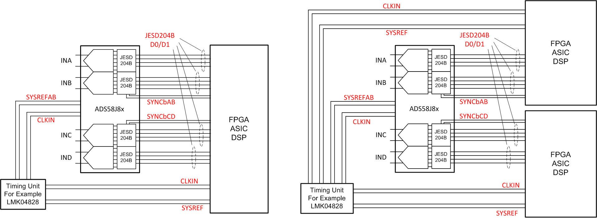 Figure 47. Four Channel and Dual Two Channel Usage
Split Mode Operation: If the ADS58J89 device is operated with 2-channel output at 500 MSPS and 2-channel output at 250 MSPS, then dual SYSREF (SYSREFAB for channel A and B, SYSREFCD for channel C and D) as well as dual SYNC (SYNCbAB for channel A and B, SYNCbCD for channel C and D) is required to ensure normal operation because the JESD204B link configuration is different for the two channel pairs.
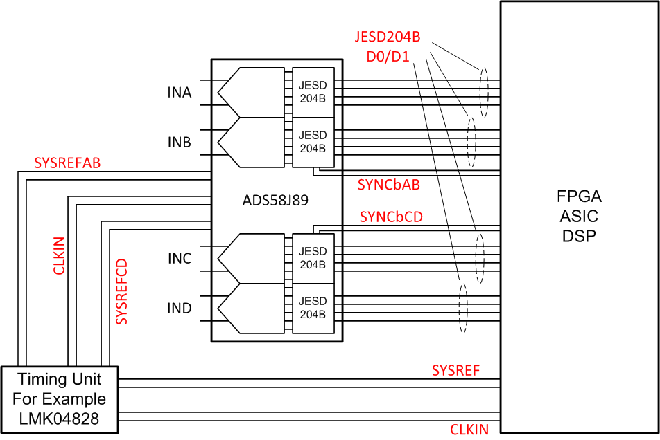 Figure 48. Dual SYSREF Usage
7.3.6 Eye Diagram Information
Figure 49 and Figure 50 is the measured eye diagram at 2.5 and 5Gbps output data rate, respectively. These are overlaid with the JESD204B LV-OIF-6G-SR specification.
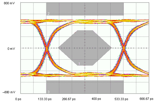 Figure 49. 2.5 Gbps Eye Diagram
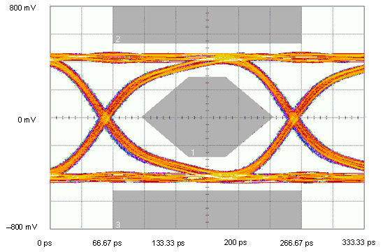 Figure 50. 5.0 Gbps Eye Diagram
7.3.7 Analog Inputs
The ADS58J89 analog signal inputs are designed to be driven differentially. The analog input pins have internal analog buffers that drive the sampling circuit. As a result of the analog buffer, the input pins present a high-impedance input across a very-wide frequency range to the external driving source, which enables great flexibility in the external analog filter design as well as excellent 50-Ω matching for RF applications. The buffer also helps isolate the external driving circuit from the internal switching currents of the sampling circuit, which results in a more constant SFDR performance across input frequencies.
The common-mode voltage of the signal inputs is internally biased to 2 V using 500-Ω resistors, which allows for AC coupling of the input drive network. Each input pin (INP, INM) must swing symmetrically between (VCM + 0.3125 V) and (VCM – 0.3125 V), resulting in a 1.25-Vpp (default) differential input swing. The input sampling circuit has a 3-dB bandwidth that extends up to 900 MHz.
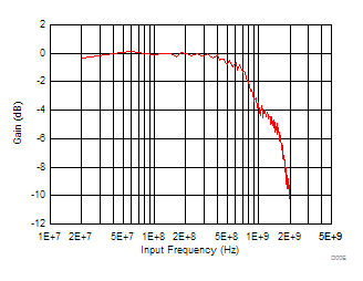 Figure 51. Normalized Input Bandwidth
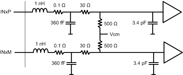 Figure 52. Equivalent Analog Input Circuit
7.3.8 Clock Inputs
The ADS58J89 clock input can be driven differentially with a sine wave or LVPECL source with little or no difference in performance. The common mode voltage of the clock input is set to 0.9 V using internal 2-kΩ resistors. This allows for AC coupling of the clock inputs. The termination resistors should be placed as close as possible to the clock inputs in order to minimize signal reflections and jitter degradation.
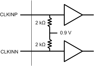 Figure 53. Equivalent Clock Input Circuit
7.3.9 Input Clock Divider
The ADS58J89 is equipped with two internal dividers on the clock input – one on channel AB and one on channel CD. The clock divider allows operation with a faster input clock simplifying the system clock distribution design. The clock dividers can be bypassed (/1) for operation with a 500-MHz clock while /2 option supports a maximum input clock of 1 GHz and the /4 option a maximum input clock frequency of 2 GHz. Different divider options can be selected for channel AB and channel CD clock output. By default the divider output of channel AB block is routed to all 4 channels but the configuration can be customized with different SPI register settings to use either the channel AB or CD divider blocks for any two channels.
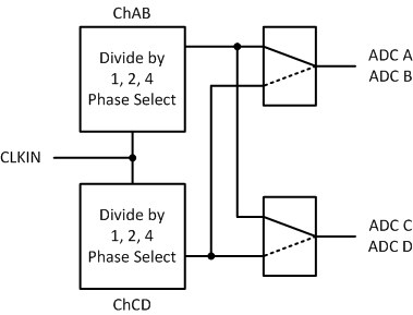 Figure 54. Input Clock Divider
7.3.10 Power-Down Control
The power down functions of the ADS58J89 can be controlled either through the parallel control pin (ENABLE) or through a SPI register setting. Power-down modes for the different channels as well as for the JESD204B interface are supported.
The ADS58J89 supports the following power-down modes. The analog sleep mode configurations are in register 0x05/06 and the JESD204b sleep mode configurations are in register 0x1E and 0x1F.
Table 4. Low-Power Mode Power Consumption and Wake-Up Times
| Configuration | Power Consumption | Wake-Up Time |
|---|---|---|
| Global power down | 24 mW | Needs JESD resynch |
| Standby | 31 mW | Needs JESD resynch |
| Deep sleep | 791 mW | 1.4 ms |
| Light sleep | 1.68 W | 8 µs |
Control power-down function through ENABLE pin:
- Configure power-down mode in register 0x05 and 0x1E
- Normal operation: ENABLE pin high
- Power-down mode: ENABLE pin low
Control power-down function through SPI (ENABLE pin always high):
- Assign power-down mode in register 0x06 and 0x1F
- Normal operation: 0x06 and 0x1F are 0xFFFF
- Power-down mode: configure power down mode in register 0x06 and 0x1F
7.3.11 Device Configuration
The serial interface (SIF) included in the ADS58J89 is a simple 3- or 4-pin interface. In normal mode, 3 pins are used to communicate with the device. There is an enable (SDENb), a clock (SCLK), and a bidirectional IO port (SDATA). If the user would like to use the 4-pin interface, one write must be implemented in the 3-pin mode to enable 4-pin communications. In this mode, the SDOUT pin becomes the dedicated output. The serial interface has an 8-bit address word and a 16-bit data word. The first rising edge of SCLK after SDENb goes low will latch the read or write bit. If a high is registered, then a read is requested, if it is low, then a write is requested. SDENb must be brought high again before another transfer can be requested.
7.3.12 JESD204B Interface Initialization Sequence
After power-up, the internal JESD204B digital block must be initialized with the following sequence of steps:
- Set JESD RESET AB/CD and JESD INIT AB/CD to 0 (address 0x0D, value 0x0000)
- Set JESD INIT AB/CD to 1 (0x0D, 0x0202)
- Set JESD RESET AB/CD to 1 (0x0D, 0x0303)
- Configure all other JESD register and clock settings. If those settings change later on, this initialization sequence must be repeated.
- Set JESD RESET AB/CD to 0 (0x0D, 0x0202)
- Set JESD RESET AB/CD to 1 (0x0D, 0x0303)
- Wait for two SYSREF pulses
- Set JESD INIT AB/CD to 0 (0x0D, 0x0101)
7.3.13 Device and Register Initialization
After power-up, the internal registers must be initialized to their default values through a hardware reset by applying a low pulse on the SRESETb pin (of width greater than 10 ns), as shown in Figure 1. If required later during operation, the serial interface registers can be cleared by applying:
- Another hardware reset using the SRESETb pin
- A software reset (bit D0 in register 0x00). This setting resets the internal registers to the default values and then self-resets the RESET bit (D0) back to 0. In this case, the RESET pin is kept high.
7.4 Device Functional Modes
7.4.1 Operating Modes
Table 5 details the five different operating modes. A pair of channels (channel A and B and channel C and D) can be configured in the same operating mode.
Table 5. Operating Modes Information
| Channel Sampling Rate (MSPS) | Digital Feature | Output Data Rate (MSPS) | Output Resolution | Output SerDes Rate (GSPS) | Number of Lanes per Channel |
|---|---|---|---|---|---|
| 500 | Decimation by 2 | 250 | 14 bit | 5.0 | 1 |
| Burst mode of every other sample | 250 | 11 to 14 bit | 5.0 | 1 | |
| 500 | SNR boost (150-MHz BW) | 500 | 9 bit | 5.0 | 2 |
| Burst mode | 500 | 9 to 14 bit | 5.0 | 2 | |
| TDD-burst mode | 500 | 9 to 14 bit | 5.0 | 2 |
7.4.2 Mode Configuration
Table 6 shows examples for different mode configurations for channel A/B and channel C/D regarding input options for SYSREF as well as the trigger for the different burst mode options. Each channel pair (A/B and C/D) can support each mode for 250-MSPS and 500-MSPS output.
Table 6. SYSREF and Trigger Options by Operating Mode
| Channel | Output Rate | Mode | SYSREF Input | Trigger Input |
|---|---|---|---|---|
| 2 | 500 MSPS | SNR boost | SYSREFAB | – |
| 2 | 500 MSPS | SNR boost | ||
| 2 | 500 MSPS | TDD burst mode | SYSREFAB | SYSREFP/M |
| 2 | 500 MSPS | TDD burst mode | OVRA/C | |
| 2 | 500 MSPS | TDD burst mode | SYSREFAB | SYSREFCDP/M |
| 2 | 500 MSPS | Burst mode | OVRA/C | |
| 2 | 500 MSPS | SNR boost | SYSREFAB | SYSREFCDP/M |
| 2 | 500 MSPS | Burst mode | OVRA/C | |
| 2 | 500 MSPS | SNR boost | SYSREFAB | OVRA/C |
| 2 | 250 MSPS | Burst mode of every other sample | SYSREFCD | |
| 2 | 500 MSPS | Burst mode | SYSREFAB | OVRA/C |
| 2 | 250 MSPS | Decimation by 2 | SYSREFCD | |
| 2 | 250 MSPS | Decimation by 2 | SYSREFAB | SYSREFCDP/M |
| 2 | 250 MSPS | Burst mode of every other sample | OVRA/C | |
| 2 | 250 MSPS | Decimation by 2 | SYSREFAB | – |
| 2 | 250 MSPS | Decimation by 2 |
7.4.3 Output Format
Table 7 provides detailed information on how the MSB or LSB get aligned for the different output data rates and resolution in the different operating modes.
Table 7. Output Data Formats
| Function | Output Rate | Mode | Resolution | Bit 15 | Bit 14 | Bit 13 | Bit 12 | Bit 11 | Bit 10 | Bit 9 | Bit 8 | Bit 7 | Bit 6 | Bit 5 | Bit 4 | Bit 3 | Bit 2 | Bit 1 | Bit 0 |
|---|---|---|---|---|---|---|---|---|---|---|---|---|---|---|---|---|---|---|---|
| RX | 250 MSPS | Decimate by 2 | 14 bit | D13 | D12 | D11 | D10 | D9 | D8 | D7 | D6 | D5 | D4 | D3 | D2 | D1 | D0 | OVR | 0 |
| FB | 250 MSPS | Burst Mode | 14 bit | D13 | D12 | D11 | D10 | D9 | D8 | D7 | D6 | D5 | D4 | D3 | D2 | D1 | D0 | OVR | HRES |
| RX | 500 MSPS | SNR Boost | 9 bit | D8 | D7 | D6 | D5 | D4 | D3 | D2 | D1 | D0 | 0 | 0 | 0 | 0 | 0 | OVR | 0 |
| FB | 500 MSPS | Burst Mode | 11 bit | D10 | D9 | D8 | D7 | D6 | D5 | D4 | D3 | D2 | D1 | D0 | 0 | 0 | 0 | OVR | HRES |
| 12 bit | D11 | D10 | D9 | D8 | D7 | D6 | D5 | D4 | D3 | D2 | D1 | D0 | 0 | 0 | OVR | HRES | |||
| 14 bit | D13 | D12 | D11 | D10 | D9 | D8 | D7 | D6 | D5 | D4 | D3 | D2 | D1 | D0 | OVR | HRES |
7.4.4 Burst Mode of Every Other Sample (250 MSPS Output)
In this mode, the channel is sampling at full sampling rate but the output only transmits every other sample with burst mode. During burst mode operation the output is alternated between low resolution 11-bit and high resolution 12- or 14-bit output. The burst mode operation can be configured to auto or manual trigger (see Burst Mode).
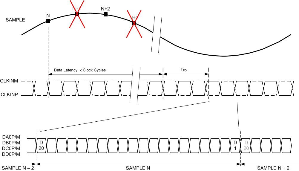 Figure 55. Timing Diagram Burst Mode of Every Other Sample
7.4.5 SNR Boost (500 MSPS Output)
In this mode, the channel output data is truncated to 9-bit resolution and the quantization noise is shaped using TI SNR Boost 3G technology. The SNR Boost passband bandwidth maximum is 150 MHz at 500 MSPS centered at the mid-point of the Nyquist zone.
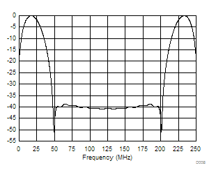 Figure 56. SNR Boost Noise Shape Response
7.4.6 Burst Mode
The ADS58J89 supports TI’s next generation burst mode technology which can be used for the DPD feedback path as well for the receive path (TDD burst mode) in TDD applications. In receive mode, the TDD burst mode is used to support very wide band and high resolution or duty cycle operation. Both modes can also be used simultaneously where two channels operate in burst mode and two channels in TDD burst mode.
In burst mode operation, the ADS58J89 alternatively transmits low resolution (11 bit for 250 MSPS operation and 9 bit for 500 MSPS operation, LSBs are set to 0) and high resolution (11-, 12-, or 14-bit) output data and can be configured via SPI register writes. The number of low and high resolution samples is configured through programmable counters.
7.4.6.1 Burst Mode Counters
The ADS58J89 provides eight independent counters each for channel A and B and channel C and D for burst mode operation. The TDD burst mode employs all eight counters (four for the low resolution samples and four for the high resolution samples) while the normal burst mode uses only H1 and L1. Each count corresponds to four samples and each counter can be programmed through a 22-bit register entry (1 to 4194303).
The counter values can be updated at any time, but the update does not go into effect until the start of the next burst mode cycle with low resolution output data (L1). After programming the counters, the ADS58J89 calculates the corresponding duty cycle for the selected high resolution output. If the duty cycle violates the limits, the digital outputs are limited to low resolution output.
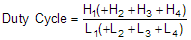
The duty cycle limits per selected high resolution output is shown in Table 8.
Table 8. Burst Mode Maximum Allowed Duty Cycle
| Maximum Allowed Duty Cycle (High : Low Resolution Output) |
500 MSPS | 250 MSPS |
|---|---|---|
| 14 bit | 1/3 | 1/1 |
| 12 bit | 2/3 | 4/1 |
| 11 bit | 3/2 | – |
7.4.6.2 Burst Mode
The number of high and low resolution samples is H1 × 22 and L1 × 22. The maximum number of low resolution samples is 22 × 222 = 224 while the maximum number of high resolution samples depends on the duty cycle.
7.4.6.3 TDD Burst Mode
The number of high and low resolution samples per cycle is (H1 + H2 + H3 + H4) × 22 and (L1 + L2 + L3 + L4) × 22.
In TDD burst mode, the output data gets transmitted in the following order:
L1, H1, L2, H2, L3, H3, L4, H4, L1, H1, and so forth
7.4.6.4 Trigger Input
The burst mode can be operated in auto trigger or manual trigger mode while the TDD burst mode supports only the manual trigger mode.
In manual trigger mode, the trigger input releases the first high resolution data (H1) burst after the low resolution data counter L1 has timed out. The OVRB outputs can be configured via SPI (address 0x6F) as output flags TRDY for channel A and B. The OVRD outputs can be configured via SPI (address 0x6F) as output flags TRDY for channel C and D. Both these configurations indicate that counter L1 timed out and the high resolution output data burst can be triggered.
The ADS58J89 provides a lot of flexibility for the configuration of the trigger input. In default operation, the single-ended input pin TRIGGERAB controls all four channels. Alternatively, the trigger input can be changed to the OVRA pin as single-ended input or as a differential input with TRIGGERAB as positive and TRIGGERCD as negative input (differential input requires external 100-Ω termination).
For simultaneous receive and DPD feedback applications, it may be more useful to split the control where the TRIGGERAB or OVRA pin controls channel A and B and the TRIGGERCD or OVRC pin controls channel C and D. In addition, the OVRB and OVRD pins can be configured to output the TRDY flag for channel A and B and channel C and D, respectively.
The trigger input for channel A/B and channel C/D can each be selected with 2 register bits (address 0x2C and 0x3A) as shown in Table 9.
Table 9. Burst Mode Trigger Sources
| Register Setting | Trigger Source |
|---|---|
| 00 | TRIGGERAB (= pin SYSREFCDP) |
| 01 | TRIGGERCD (= pin SYSREFCDM) |
| 10 | OVRA (for channel A/B) OVRC (for channel C/D) |
| 11 | TRIGGERAB/CD (as differential LVDS input, single trigger input for all 4 channels) |
7.4.6.5 Manual Trigger Mode
Upon enabling manual trigger mode, the ADS58J89 starts transmission of low resolution data. As soon as the L1 counter is finished, the manual trigger is unlocked and the high resolution output H1 or burst mode sequence of H1, L2, H2, L3, H3, L4, H4, L1 can be triggered. After the low resolution counter L1 is finished, the next high resolution output or burst mode sequence can be triggered again. The HRES flag is embedded in the JESD204B output data stream. The counter values can be updated until a new burst mode cycles starts with transmission of low resolution samples.
See Figure 57 for an example of normal burst mode with manual trigger.
 Figure 57. Burst Mode Duty Cycle Timing
See Figure 58 for an example of TDD burst mode with manual trigger:
 Figure 58. TDD Burst Mode Duty Cycle Timing
7.4.6.6 Auto Trigger Mode
This mode is primarily intended for the DPD observation path. Upon enabling auto trigger mode, the ADS58J89 starts transmission of low resolution data. As soon as the L1 counter is finished, the ADS58J89 immediately begins transmitting the high resolution output H1. The HRES flag can also be embedded in the JESD204B output data stream. The counter values can be updated until a new burst mode cycles starts with transmission of low resolution samples. Any input on the trigger input pins is ignored.
See Figure 59 for an example of normal burst mode with automatic trigger:
 Figure 59. Auto-Trigger Mode Duty Cycle Timing
7.4.6.7 TDD-Burst Mode
This mode is intended for the receive path in TDD LTE receivers. The individual counters for high and low resolution output data can be programmed so that the high resolution samples line up with receive (uplink) frames and the low resolution samples line up with transmit (downlink) and setup frames where no data is present in the receive path.
Table 10. TDD Burst Mode Duty Cycle
| Option | Number of Setup Frames | Number of Downlink Frames | Number of Uplink Frames | Duty Cycle | High Resolution Output (500 MSPS) |
|---|---|---|---|---|---|
| 1 | 1 | 8 | 1 | 1:9 (0.11) | 14 bit |
| 2 | 7 | 2 | 2:8 (0.25) | 14 bit | |
| 3 | 6 | 3 | 3:7 (0.43) | 12 bit | |
| 4 | 5 | 4 | 4:6 (0.67) | 11/12 bit | |
| 5 | 1 to 4 | 5 to 8 | (1+) | 11 bit | |
| 6 | 2 | 6 | 2 | 2:8 (0.25) | 14 bit |
| 7 | 5 | 3 | 3:7 (0.43) | 12 bit | |
| 8 | 4 | 4 | 4:6 (0.67) | 11/12 bit | |
| 9 | 1 to 3 | 5 to 7 | >1 | 11 bit |
7.4.6.7.1 TDD Burst Mode Examples
Following are two examples to illustrate the intention for the TDD burst mode. The TDD frame has 10 equal size sub frames. For the downlink-uplink (DL-UL) configuration number 2 for example, the high and low resolution counters can be set for a given channel sampling rate to match the downlink-uplink profile as shown in Figure 60. The manual trigger is used to initiate the high resolution output data, which maintains synchronization. The counter L1 covers the low resolution data across two consecutive TDD frames and most of setup frame.
For configuration number 2, a duty cycle of approximately 2 / 8 can be achieved; with a sampling rate of 500 MSPS, the high resolution output of 14 bit can be used.
 Figure 60. TDD Burst Mode Example 1
For configuration number 3, a duty cycle of approximately 3 / 7 can be achieved and only two counters have to be programmed. With a sampling rate of 500 MSPS, a high resolution output of 12 bit can be used.
 Figure 61. TDD Burst Mode Example 2
7.5 Programming
7.5.1 Serial Register Write
The internal register of the ADS58J89 can be programmed following these steps:
- Drive SDENb pin low.
- Set the R/W bit to ‘0’ (bit A7 of the 8 bit address).
- Initiate a serial interface cycle specifying the address of the register (A6 to A0) whose content has to be written.
- Write 16-bit data which is latched on the rising edge of SCLK.
Table 11. Serial Register Read or Write Timing(1)
| PARAMETER | MIN | TYP | MAX | UNIT | |
|---|---|---|---|---|---|
| ƒSCLK | SCLK frequency (equal to 1 / tSCLK) | >DC | 10 | MHz | |
| tSLOADS | SDENb to SCLK setup time | 50 | ns | ||
| tSLOADH | SCLK to SDENb hold time | 50 | ns | ||
| tDSU | SDATA setup time | 50 | ns | ||
| tDH | SDATA hold time | 50 | ns | ||
 Figure 62. Serial Register Write Timing Diagram
7.5.2 Serial Register Readout
The device includes a mode where the contents of the internal registers can be read back using the SDOUT and SDATA pins. This read-back mode may be useful as a diagnostic check to verify the serial interface communication between the external controller and the channel.
- Drive SDENb pin low.
- Set the RW bit (A7) to 1. This setting disables any further writes to the registers.
- Initiate a serial interface cycle specifying the address of the register (A6 to A0) whose content has to be read.
- The device outputs the contents (D15 to D0) of the selected register on the SDOUT/SDATA pin.
- The external controller can latch the contents at the SCLK rising edge.
- To enable register writes, reset the RW register bit to 0.
 Figure 63. Serial Register Read Timing Diagram
7.6 Register Maps
| Register Address | Register Data | |||||||||||||||
|---|---|---|---|---|---|---|---|---|---|---|---|---|---|---|---|---|
| A7 to A0 in hex | D15 | D14 | D13 | D12 | D11 | D10 | D9 | D8 | D7 | D6 | D5 | D4 | D3 | D2 | D1 | D0 |
| 0 | 3/4 WIRE | FORMAT | DEC EN AB | HP/LP AB | 0 | DEC EN CD | HP/LP CD | 0 | SNRB EN AB | SNRB EN CD | 0 | 0 | 0 | 0 | 0 | RESET |
| 1 | MODE 1 | 0 | 1 | 0 | FOVR THRESH AB | FOVR LENGTH AB | FOVR THRESH CD | FOVR LENGTH CD | 1 | 0 | ||||||
| 2 | 0 | 1 | BM RES | DISCARD AB | DISCARD CD | 0 | 0 | 0 | 0 | 0 | 0 | 0 | 0 | 0 | 0 | |
| 3 | 0 | CLK SEL CD | CLK DIV CD | 0 | CLK PHASE SELECT CD | SYSREF SEL CD | CLK SEL AB | CLK DIV AB | 0 | CLK PHASE SELECT AB | ||||||
| 4 | OVRA OUT EN | OVRB OUT EN | OVRC OUT EN | OVRD OUT EN | SYSREF AB DELAY | SYSREF CD DELAY | 0 | 0 | 0 | 0 | SYNCb AB EN | SYNCb CD EN | 1 | 1 | ||
| 5 | ANALOG SLEEP MODES – ENABLE PIN | |||||||||||||||
| 6 | ANALOG SLEEP MODES – SPI | SYSREFCD EN | ||||||||||||||
| 7 | 0 | 0 | 0 | 0 | 0 | 0 | CLK SW AB | 1 | 0 | 1 | 0 | 0 | 0 | 1 | 0 | 0 |
| 8 | 0 | 0 | 0 | 0 | 0 | 0 | CLK SW CD | 1 | 0 | 1 | 0 | 0 | 0 | 1 | 0 | 0 |
| C | 0 | 0 | 1 | 1 | 0 | 0 | 0 | 1 | 1 | 1 | SYSREF JESD MODE CD | SYSREF JESD MODE AB | ||||
| D | 0 | 0 | 0 | 0 | 0 | 0 | JESD INIT CD | JESD RESET CD | 0 | 0 | 0 | 0 | 0 | 0 | JESD INIT AB | JESD RESET AB |
| E | 0 | 0 | 0 | 0 | 0 | 0 | 0 | 0 | TX LANE EN CD | TX LANE EN AB | ||||||
| F | 0 | 0 | 0 | 0 | 0 | 0 | CTRL F AB | 0 | 0 | 0 | 0 | 0 | 0 | CTRL M AB | ||
| 10 | 0 | 0 | 0 | 0 | 0 | 0 | CTRL K AB | 0 | 0 | 0 | CTRL L AB | |||||
| 13 | 0 | 0 | 0 | 0 | 0 | 0 | 0 | 0 | 0 | INV SYNCb AB | HD AB | SCR EN AB | 0 | 0 | 0 | 0 |
| 16 | 0 | 0 | 0 | 0 | 0 | 0 | CTRL F CD | 0 | 0 | 0 | 0 | 0 | 0 | CTRL M CD | ||
| 17 | 0 | 0 | 0 | 0 | 0 | 0 | CTRL K CD | 0 | 0 | 0 | CTRL L CD | |||||
| 1A | 0 | 0 | 0 | 0 | 0 | 0 | 0 | 0 | 0 | INV SYNCb CD | HD CD | SCR EN CD | 0 | 0 | 0 | 0 |
| 1D | 0 | 0 | 0 | 0 | 0 | 0 | 0 | 0 | 0 | TEST PATTERN EN CD | TEST PATTERN EN AB | 0 | TEST PATTERN | 0 | 0 | 0 |
| 1E | 0 | 0 | 0 | 0 | 0 | 0 | JESD SLEEP MODES – ENABLE PIN | |||||||||
| 1F | 1 | 1 | 1 | 1 | 1 | 1 | JESD SLEEP MODES – SPI | |||||||||
| 20 | JESD LANE POLARITY INVERT | PRBS EN | ||||||||||||||
| 21 | 0 | PRBS SEL | 0 | 0 | 0 | 0 | 0 | 0 | 0 | 0 | 0 | 0 | VREF SEL | |||
Table 12.
| Register Address | Register Data | |||||||||||||||
|---|---|---|---|---|---|---|---|---|---|---|---|---|---|---|---|---|
| A7 to A0 in hex | D15 | D14 | D13 | D12 | D11 | D10 | D9 | D8 | D7 | D6 | D5 | D4 | D3 | D2 | D1 | D0 |
| 24 | TDD BURST MODE COUNTER L1 [15:0] AB | |||||||||||||||
| 25 | TDD BURST MODE COUNTER L2 [15:0] AB | |||||||||||||||
| 26 | TDD BURST MODE COUNTER L3 [15:0] AB | |||||||||||||||
| 27 | TDD BURST MODE COUNTER L4 [15:0] AB | |||||||||||||||
| 28 | TDD BURST MODE COUNTER H1 [15:0] AB | |||||||||||||||
| 29 | TDD BURST MODE COUNTER H2 [15:0] AB | |||||||||||||||
| 2A | TDD BURST MODE COUNTER H3 [15:0] AB | |||||||||||||||
| 2B | TDD BURST MODE COUNTER H4 [15:0] AB | |||||||||||||||
| 2C | BM TRIG AB | TDD BURST MODE COUNTER L2 [21:16] AB | 0 | 0 | TDD BURST MODE COUNTER L1 [21:16] AB | |||||||||||
| 2D | 0 | 0 | TDD BURST MODE COUNTER L4 [21:16] AB | 0 | 0 | TDD BURST MODE COUNTER L3 [21:16] AB | ||||||||||
| 2E | 0 | 0 | TDD BURST MODE COUNTER H2 [21:16] AB | 0 | 0 | TDD BURST MODE COUNTER H1 [21:16] AB | ||||||||||
| 2F | AUTO TRIG AB | TDD EN AB | TDD BURST MODE COUNTER H4 [21:16] AB | 0 | 0 | TDD BURST MODE COUNTER H3 [21:16] AB | ||||||||||
| 32 | TDD BURST MODE COUNTER L1 [15:0] CD | |||||||||||||||
| 33 | TDD BURST MODE COUNTER L2 [15:0] CD | |||||||||||||||
| 34 | TDD BURST MODE COUNTER L3 [15:0] CD | |||||||||||||||
| 35 | TDD BURST MODE COUNTER L4 [15:0] CD | |||||||||||||||
| 36 | TDD BURST MODE COUNTER H1 [15:0] CD | |||||||||||||||
| 37 | TDD BURST MODE COUNTER H2 [15:0] CD | |||||||||||||||
| 38 | TDD BURST MODE COUNTER H3 [15:0] CD | |||||||||||||||
| 39 | TDD BURST MODE COUNTER H4 [15:0] CD | |||||||||||||||
| 3A | BM TRIG CD | TDD BURST MODE COUNTER L2 [21:16] CD | 0 | 0 | TDD BURST MODE COUNTER L1 [21:16] CD | |||||||||||
| 3B | 0 | 0 | TDD BURST MODE COUNTER L4 [21:16] CD | 0 | 0 | TDD BURST MODE COUNTER L3 [21:16] CD | ||||||||||
| 3C | 0 | 0 | TDD BURST MODE COUNTER H2 [21:16] CD | 0 | 0 | TDD BURST MODE COUNTER H1 [21:16] CD | ||||||||||
| 3D | AUTO TRIG CD | TDD EN CD | TDD BURST MODE COUNTER H4 [21:16] CD | 0 | 0 | TDD BURST MODE COUNTER H3 [21:16] CD | ||||||||||
| 63 | 0 | 0 | 0 | 0 | 0 | 0 | 0 | TEMP SENSOR | ||||||||
| 64 | PRE EMP SEL AB | PRE EMP EN AB | DCC EN AB | 0 | 0 | 0 | 0 | |||||||||
| 67 | OUTPUT CURRENT CONTROL AB | |||||||||||||||
| 68 | PRE EMP SEL CD | PRE EMP EN CD | DCC EN CD | 0 | 0 | 0 | 0 | |||||||||
| 6B | OUTPUT CURRENT CONTROL CD | |||||||||||||||
| 6C | 0 | 0 | 0 | 0 | 0 | 0 | 0 | 0 | 0 | 0 | TDD RATIO CD | TDD RATIO AB | BM RATIO CD | BM RATIO AB | JESD PLL CD | JESD PLL AB |
| 6F | 0 | 0 | 0 | 0 | 0 | 0 | 0 | 0 | 0 | TRDY EN AB | 0 | 0 | 0 | 0 | 0 | TRDY EN CD |
7.6.1 Register Descriptions
7.6.1.1 Register Address 0
| D15 | D14 | D13 | D12 | D11 | D10 | D9 | D8 | D7 | D6 | D5 | D4 | D3 | D2 | D1 | D0 |
|---|---|---|---|---|---|---|---|---|---|---|---|---|---|---|---|
| 3/4 WIRE | FORMAT | DEC EN AB | HP/LP AB | 0 | DEC EN CD | HP/LP CD | 0 | SNRB EN AB | SNRB EN CD | 0 | 0 | 0 | 0 | 0 | RESET |
| LEGEND: R/W = Read/Write; R = Read only; -n = value after reset |
Table 13. Register Address 0 Field Descriptions
| Bit | Field | Type | Reset | Description |
|---|---|---|---|---|
| D15 | 3/4 WIRE | Enables 4-bit serial interface when set 0 = 3-wire SPI (SDATA is bidirectional) 1 = 4-wire SPI (SDOUT is data output) |
||
| D14 | FORMAT | Selects digital output format 0 = Output is 2s complement 1 = Offset binary |
||
| D13 | DEC EN AB | Enables decimation filter for channel AB 0 = Normal operation 1 = Decimation filter enabled |
||
| D12 | HP/LP AB | Determines high-pass or low-pass configuration of decimation filter for channel AB 0 = Low pass 1 = High pass |
||
| D10 | DEC EN CD | Enables decimation filter for channel CD 0 = Normal operation 1 = Decimation filter enabled |
||
| D9 | HP/LP CD | Determines high-pass or low-pass configuration of decimation filter for channel CD 0 = Low pass 1 = High pass |
||
| D7 | SNRB EN AB | Enables SNR boost for channel AB 0 = Normal operation 1 = SNR boost enabled |
||
| D6 | SNRB EN CD | Enables SNR boost for channel CD 0 = Normal operation 1 = SNR boost enabled |
||
| D0 | RESET | Software reset, self clears to 0 0 = Normal operation 1 = Execute software reset |
7.6.1.2 Register Address 1
| D15 | D14 | D13 | D12 | D11 | D10 | D9 | D8 | D7 | D6 | D5 | D4 | D3 | D2 | D1 | D0 |
|---|---|---|---|---|---|---|---|---|---|---|---|---|---|---|---|
| MODE 1 | 0 | 1 | 0 | FOVR THRESH AB | FOVR LENGTH AB | FOVR THRESH CD | FOVR LENGTH CD | 1 | 0 | ||||||
| LEGEND: R/W = Read/Write; R = Read only; -n = value after reset |
Table 14. Register Address 1 Field Descriptions
| Bit | Field | Type | Reset | Description |
|---|---|---|---|---|
| D15 | MODE 1 | Set bit D15 to 0 for optimum performance | ||
| D13 | Reads back 1 | |||
| D11:D9 | FOVR THRESH AB | Sets fast OVR thresholds for channel A and B The fast over-range detection is triggered 6 output clock cycles after the overload condition occurs. The threshold at which the OVR is triggered is: Input full scale × [decimal value of <over-range threshold>] / 8. After power-up or reset, the default value is 7 (decimal), which corresponds to an OVR threshold of 1.16-dB below full scale (20 × log(7/8)).  Figure 66. OVR Detection Threshold Figure 66. OVR Detection Threshold
|
||
| D8:D7 | FOVR LENGTH AB | Determines minimum pulse length for FOVR output 00 = 1 clock cycle 01 = 2 clock cycles 10 = 4 clock cycles 11 = 8 clock cycles |
||
| D6:D4 | FOVR THRESH CD | Sets fast OVR thresholds for channel C and D See description for channel A and B | ||
| D3:D2 | FOVR LENGTH CD | Determines minimum pulse length for FOVR output 00 = 1 clock cycle 01 = 2 clock cycles 10 = 4 clock cycles 11 = 8 clock cycles |
||
| D1 | Reads back 1 |
7.6.1.3 Register Address 2
| D15 | D14 | D13 | D12 | D11 | D10 | D9 | D8 | D7 | D6 | D5 | D4 | D3 | D2 | D1 | D0 |
|---|---|---|---|---|---|---|---|---|---|---|---|---|---|---|---|
| 0 | 1 | BM RES | DISCARD AB | DISCARD CD | 0 | 0 | 0 | 0 | 0 | 0 | 0 | 0 | 0 | 0 | |
| LEGEND: R/W = Read/Write; R = Read only; -n = value after reset |
Table 15. Register Address 2 Field Descriptions
| Bit | Field | Type | Reset | Description |
|---|---|---|---|---|
| D14 | Reads back 1 | |||
| D13:D12 | BM RES | Sets high resolution output for burst mode and TDD burst mode 00 = 14-bit high resolution output 01 = 12-bit high resolution output 10 = 11-bit high resolution output 11 = 9-bit high resolution output (in 500-MSPS operation, burst mode is disabled) |
||
| D11 | DISCARD AB | Outputs every other sample with 11-bit resolution for channel A and B. Burst mode is used if output resolution is set to 12 or 14 bit (bit D13 to D12). 0 = Normal operation 1 = Discard mode enabled |
||
| D10 | DISCARD CD | Outputs every other sample with 11-bit resolution for channel C and D. Burst mode is used if output resolution is set to 12 or 14 bit (bit D13 to D12). 0 = Normal operation 1 = Discard mode enabled |
7.6.1.4 Register Address 3
| D15 | D14 | D13 | D12 | D11 | D10 | D9 | D8 | D7 | D6 | D5 | D4 | D3 | D2 | D1 | D0 |
|---|---|---|---|---|---|---|---|---|---|---|---|---|---|---|---|
| 0 | CLK SEL CD | CLK DIV CD | 0 | CLK PHASE SELECT CD | SYSREF SEL CD | CLK SEL AB | CLK DIV AB | 0 | CLK PHASE SELECT AB | ||||||
| LEGEND: R/W = Read/Write; R = Read only; -n = value after reset |
Table 16. Register Address 3 Field Descriptions
| Bit | Field | Type | Reset | Description |
|---|---|---|---|---|
| D14 | CLK SEL CD | Clock source selection for channel C and D 0 = Channel CD clock output divider 1 = Channel AB clock output divider (default) |
||
| D13:D12 | CLK DIV CD | Channel CD clock divider setting 00 = Clock input is up to 500 MHz. Input clock is not divided (default) 01 = /2 10 = /4 11 = Not used |
||
| D10:D8 | CLK PHASE SELECT CD | Selects phase of channel divided clock, but depends on clock divider setting. When clock CD divider is set to: /1 = 2 phases are available (0º or 180º) /2 = 4 phases are available (0º, 90º, 180º or 270º) /4 = 8 phases are available (0º, 45º, 90º, 135º, 180º, 225º, 270º or 315º) When switching clock phases, register 0x08, D9 must be enabled first and then disabled after the switch to ensure glitch-free operation. |
||
| D7 | SYSREF SEL CD | SYSREF Input selection for channel C and D 0 = Use SYSREFAB inputs (default) 1 = Use SYSREFCD inputs |
||
| D6 | CLK SEL AB | Clock source selection for channel A and B 0 = Channel CD clock output divider 1 = Channel AB clock output divider (default) |
||
| D5:D4 | CLK DIV AB | Channel AB clock divider setting 00 = Clock input is up to 500 MHz. Input clock is not divided (default) 01 = /2 10 = /4 11 = Not used |
||
| D2:D0 | CLK PHASE SELECT AB | Selects phase of channel AB divided clock, but depends on clock divider setting. When clock divider is set to: /1 = 2 phases are available (0º or 180º) /2 = 4 phases are available (0º, 90º, 180º or 270º) /4 = 8 phases are available (0º, 45º, 90º, 135º, 180º, 225º, 270º or 315º) When switching clock phases, register 0x07, D9 must be enabled first and then disabled after the switch to ensure glitch-free operation. |
7.6.1.5 Register Address 4
| D15 | D14 | D13 | D12 | D11 | D10 | D9 | D8 | D7 | D6 | D5 | D4 | D3 | D2 | D1 | D0 |
|---|---|---|---|---|---|---|---|---|---|---|---|---|---|---|---|
| OVRA OUT EN | OVRB OUT EN | OVRC OUT EN | OVRD OUT EN | SYSREF AB DELAY | SYSREF CD DELAY | 0 | 0 | 0 | 0 | SYNCb AB EN | SYNCb CD EN | 1 | 1 | ||
| LEGEND: R/W = Read/Write; R = Read only; -n = value after reset |
Table 17. Register Address 4 Field Descriptions
| Bit | Field | Type | Reset | Description |
|---|---|---|---|---|
| D15 | OVRA OUT EN | OVRA pin output enable 0 = OVRA is an input for burst mode trigger (see register 0x2C) 1 = OVRA is an output |
||
| D14 | OVRB OUT EN | OVRB pin output enable 0 = Not used (default) 1 = OVRB is an output |
||
| D13 | OVRC OUT EN | OVRC pin output enable 0 = OVRC is an input for burst mode trigger (see register 0x3A) 1 = OVRC is an output |
||
| D12 | OVRD OUT EN | OVRD pin output enable 0 = Not used (default) 1 = OVRD is an output |
||
| D11:D10 | SYSREF AB DELAY | Programmable input delay on SYSREFAB input 00 = 0-ps delay (default) 01 = 200-ps delay 10 = 100-ps delay 11 = 300-ps delay |
||
| D9:D8 | SYSREF CD DELAY | Programmable input delay on SYSREFCD input 00 = 0-ps delay (default) 01 = 200-ps delay 10 = 100-ps delay 11 = 300-ps delay |
||
| D3 | SYNCb AB EN | SYNCbAB input buffer enable 0 = Input buffer disabled 1 = Input buffer enabled (default) |
||
| D2 | SYNCb CD EN | SYNCbCD input buffer enable 0 = Input buffer disabled 1 = Input buffer enabled (default) |
||
| D1 | Reads back 1 | |||
| D0 | Reads back 1 |
7.6.1.6 Register Address 5
| D15 | D14 | D13 | D12 | D11 | D10 | D9 | D8 | D7 | D6 | D5 | D4 | D3 | D2 | D1 | D0 |
|---|---|---|---|---|---|---|---|---|---|---|---|---|---|---|---|
| ANALOG SLEEP MODES – ENABLE pin | |||||||||||||||
| LEGEND: R/W = Read/Write; R = Read only; -n = value after reset |
Table 18. Register Address 5 Field Descriptions
| Bit | Field | Type | Reset | Description |
|---|---|---|---|---|
| D15:D0 | ANALOG SLEEP MODES – ENABLE pin | Power-down function assigned to ENABLE pin. When any bit is set, the corresponding function is always enabled regardless of status of the ENABLE pin. This assumes address 0x06 is in default configuration. | ||
| D13 | Light sleep channel A | |||
| D11 | Light sleep channel B | |||
| D9 | Light sleep channel C | |||
| D7 | Light sleep channel D | |||
| D6 | Temperature sensor | |||
| D4 | Clock buffer | |||
| D3 | Clock divider channel AB | |||
| D2 | Clock divider channel CD | |||
| D1 | Buffer SYSREFAB | |||
| D0 | Buffer SYSREFCD |
Table 19. Configurations When ENABLE Pin is Low
| Description | |
|---|---|
| 0000 0000 0000 0000 | Global power down |
| 1000 0000 0000 0000 | Standby |
| 1000 0000 0001 1111 | Deep sleep |
| 1010 1010 1001 1111 | Light sleep (if unused, clock divider CD and SYSREFCD can be set to 0 also) |
7.6.1.7 Register Address 6
| D15 | D14 | D13 | D12 | D11 | D10 | D9 | D8 | D7 | D6 | D5 | D4 | D3 | D2 | D1 | D0 |
|---|---|---|---|---|---|---|---|---|---|---|---|---|---|---|---|
| ANALOG SLEEP MODES – SPI | SYSREFCD EN | ||||||||||||||
| LEGEND: R/W = Read/Write; R = Read only; -n = value after reset |
Table 20. Register Address 6 Field Descriptions
| Bit | Field | Type | Reset | Description |
|---|---|---|---|---|
| D15:D1 | ANALOG SLEEP MODES – SPI | Power-down function controlled via SPI. When a bit is set to 0, the function is powered down when ENABLE pin is high. However, register 0x05 has higher priority. For example, if D13 (deep sleep channel A) in 0x05 is enabled, it cannot be powered down with the SPI. | ||
| D13 | Light sleep channel A | |||
| D11 | Light sleep channel B | |||
| D9 | Light sleep channel C | |||
| D7 | Light sleep channel D | |||
| D6 | Temperature sensor | |||
| D4 | Clock buffer | |||
| D3 | Clock divider channel AB | |||
| D2 | Clock divider channel CD | |||
| D1 | Buffer SYSREFAB | |||
| D0 | SYSREFCD EN | Enables SYSREFCD input for dual SYSREF operation 0 = TRIGGER input for burst mode (differential or single ended, see address 0x2C/3A) 1 = SYSREF input for channel C/D (default) |
Table 21. Configurations When ENABLE Pin is High
| Description | |
|---|---|
| 0000 0000 0000 000 | Global power down |
| 1000 0000 0000 000 | Standby |
| 1000 0000 0001 111 | Deep sleep |
| 1010 1010 1001 111 | Light sleep |
| 1111 1111 1111 111 | Normal operation |
Control power down function through ENABLE pin:
- Configure power-down mode in register 0x05
- Normal operation: ENABLE pin high
- Power-down mode: ENABLE pin low
Control power down function through SPI (ENABLE pin always high):
- Assign power-down mode in register 0x06
- Normal operation 0x06 is 0xFFFF
- Power-down mode: configure power down mode in register 0x06
7.6.1.8 Register Address 7
| D15 | D14 | D13 | D12 | D11 | D10 | D9 | D8 | D7 | D6 | D5 | D4 | D3 | D2 | D1 | D0 |
|---|---|---|---|---|---|---|---|---|---|---|---|---|---|---|---|
| 0 | 0 | 0 | 0 | 0 | 0 | CLK SW AB | 1 | 0 | 1 | 0 | 0 | 0 | 1 | 0 | 0 |
| LEGEND: R/W = Read/Write; R = Read only; -n = value after reset |
Table 22. Register Address 7 Field Descriptions
| Bit | Field | Type | Reset | Description |
|---|---|---|---|---|
| D9 | CLK SW AB | User should set this bit to 1 when changing the clock phase of the clock divider AB. After the change is complete user needs to write this bit back to 0. | ||
| D8 | Reads back 1 | |||
| D6 | Reads back 1 | |||
| D2 | Reads back 1 |
7.6.1.9 Register Address 8
| D15 | D14 | D13 | D12 | D11 | D10 | D9 | D8 | D7 | D6 | D5 | D4 | D3 | D2 | D1 | D0 |
|---|---|---|---|---|---|---|---|---|---|---|---|---|---|---|---|
| 0 | 0 | 0 | 0 | 0 | 0 | CLK SW CD | 1 | 0 | 1 | 0 | 0 | 0 | 1 | 0 | 0 |
| LEGEND: R/W = Read/Write; R = Read only; -n = value after reset |
Table 23. Register Address 8 Field Descriptions
| Bit | Field | Type | Reset | Description |
|---|---|---|---|---|
| D9 | CLK SW CD | User should set this bit to 1 when changing the clock phase of the clock divider CD. After the change is complete user needs to write this bit back to 0. | ||
| D8 | Reads back 1 | |||
| D6 | Reads back 1 | |||
| D2 | Reads back 1 |
7.6.1.10 Register Address 12
| D15 | D14 | D13 | D12 | D11 | D10 | D9 | D8 | D7 | D6 | D5 | D4 | D3 | D2 | D1 | D0 |
|---|---|---|---|---|---|---|---|---|---|---|---|---|---|---|---|
| 0 | 0 | 1 | 1 | 0 | 0 | 0 | 1 | 1 | 1 | SYSREF JESD MODE CD | SYSREF JESD MODE AB | ||||
| LEGEND: R/W = Read/Write; R = Read only; -n = value after reset |
Table 24. Register Address 12 Field Descriptions
| Bit | Field | Type | Reset | Description |
|---|---|---|---|---|
| D13 | Reads back 1 | |||
| D12 | Reads back 1 | |||
| D8 | Reads back 1 | |||
| D7 | Reads back 1 | |||
| D6 | Reads back 1 | |||
| D5:D3 | SYSREF JESD MODE CD | Determines how SYSREF is used in the JESD block for channel CD 000 = Ignore SYSREF input 001 = Use all SYSREF pulses 010 = Use only the next SYSREF pulse 011 = Skip one SYSREF pulse then use only the next one 100 = Skip one SYSREF pulse then use all pulses (default) 101 = Skip two SYSREF pulses and then use one 111 = Skip two SYSREF pulses and then use all |
||
| D2:D0 | SYSREF JESD MODE AB | Determines how SYSREF is used in the JESD block for channel AB. Same functionality as SYSREF JESD MODE CD |
7.6.1.11 Register Address 13
| D15 | D14 | D13 | D12 | D11 | D10 | D9 | D8 | D7 | D6 | D5 | D4 | D3 | D2 | D1 | D0 |
|---|---|---|---|---|---|---|---|---|---|---|---|---|---|---|---|
| 0 | 0 | 0 | 0 | 0 | 0 | JESD INIT CD | JESD RESET CD | 0 | 0 | 0 | 0 | 0 | 0 | JESD INIT AB | JESD RESET AB |
| LEGEND: R/W = Read/Write; R = Read only; -n = value after reset |
Table 25. Register Address 13 Field Descriptions
| Bit | Field | Type | Reset | Description |
|---|---|---|---|---|
| D9 | JESD INIT CD | Puts the JESD block in INITIALIZATION state when set high. In this state the JESD parameters can be programmed and the outputs will stay at 0. See also JESD start-up sequence. | ||
| D8 | JESD RESET CD | Resets the JESD block when low | ||
| D1 | JESD INIT AB | Puts the JESD block in initialization state when set high. In this state the JESD parameters can be programmed and the outputs will stay at 0. | ||
| D0 | JESD RESET AB | Resets the JESD block when low |
7.6.1.12 Register Address 14
| D15 | D14 | D13 | D12 | D11 | D10 | D9 | D8 | D7 | D6 | D5 | D4 | D3 | D2 | D1 | D0 |
|---|---|---|---|---|---|---|---|---|---|---|---|---|---|---|---|
| 0 | 0 | 0 | 0 | 0 | 0 | 0 | 0 | TX LANE EN CD | TX LANE EN AB | ||||||
| LEGEND: R/W = Read/Write; R = Read only; -n = value after reset |
Table 26. Register Address 14 Field Descriptions
| Bit | Field | Type | Reset | Description |
|---|---|---|---|---|
| D7:D4 | TX LANE EN CD | Enables JESD204B transmitter for channel C and D. Set to 1 to enable. D7 = Lane DD1 D6 = Lane DD0 D5 = Lane DC1 D4 = Lane DC0 |
||
| D3:D0 | TX LANE EN AB | Enables JESD204B transmitter for channel A and B. Set to 1 to enable. D3 = Lane DB1 D2 = Lane DB0 D1 = Lane DA1 D0 = Lane DA0 |
7.6.1.13 Register Address 15
| D15 | D14 | D13 | D12 | D11 | D10 | D9 | D8 | D7 | D6 | D5 | D4 | D3 | D2 | D1 | D0 |
|---|---|---|---|---|---|---|---|---|---|---|---|---|---|---|---|
| 0 | 0 | 0 | 0 | 0 | 0 | CTRL F AB | 0 | 0 | 0 | 0 | 0 | 0 | CTRL M AB | ||
| LEGEND: R/W = Read/Write; R = Read only; -n = value after reset |
Table 27. Register Address 15 Field Descriptions
| Bit | Field | Type | Reset | Description |
|---|---|---|---|---|
| D9:D8 | CTRL F AB | Controls number of octets per frame for channel AB. 00 = F = 1 (default) 01 = F = 2 |
||
| D1:D0 | CTRL M AB | Controls number of converters per link for channel AB. 01 = M = 2. This is the only valid option (default) |
7.6.1.14 Register Address 16
| D15 | D14 | D13 | D12 | D11 | D10 | D9 | D8 | D7 | D6 | D5 | D4 | D3 | D2 | D1 | D0 |
|---|---|---|---|---|---|---|---|---|---|---|---|---|---|---|---|
| 0 | 0 | 0 | 0 | 0 | 0 | CTRL K AB | 0 | 0 | 0 | CTRL L AB | |||||
| LEGEND: R/W = Read/Write; R = Read only; -n = value after reset |
Table 28. Register Address 16 Field Descriptions
| Bit | Field | Type | Reset | Description |
|---|---|---|---|---|
| D9:D5 | CTRL K AB | Controls number of frames per multi-frame for channel AB. 0: K = 1 30 K = 31 1: K = 2 31 K = 32 (default) And so forth |
||
| D1:D0 | CTRL L AB | Controls number of lanes for channel AB. 01: L = 2 11: L = 4 (default) |
7.6.1.15 Register Address 19
| D15 | D14 | D13 | D12 | D11 | D10 | D9 | D8 | D7 | D6 | D5 | D4 | D3 | D2 | D1 | D0 |
|---|---|---|---|---|---|---|---|---|---|---|---|---|---|---|---|
| 0 | 0 | 0 | 0 | 0 | 0 | 0 | 0 | 0 | INV SYNCb AB | HD AB | SCR EN AB | 0 | 0 | 0 | 0 |
| LEGEND: R/W = Read/Write; R = Read only; -n = value after reset |
Table 29. Register Address 19 Field Descriptions
| Bit | Field | Type | Reset | Description |
|---|---|---|---|---|
| D6 | INV SYNCb AB | Inverts polarity of SYNCbAB input 0 = Normal operation 1 = Polarity inverted |
||
| D5 | HD AB | Enables high density mode for channel AB. This mode is needed for LMFS = 4221. 0 = High-density mode disabled for mode LMFS = 2221 1 = High-density mode enabled for mode LMFS = 4221 (default) |
||
| D4 | SCR EN AB | Enables scramble mode for channel AB 0 = Scramble mode disabled (default) 1 = Scramble mode enabled |
7.6.1.16 Register Address 22
| D15 | D14 | D13 | D12 | D11 | D10 | D9 | D8 | D7 | D6 | D5 | D4 | D3 | D2 | D1 | D0 |
|---|---|---|---|---|---|---|---|---|---|---|---|---|---|---|---|
| 0 | 0 | 0 | 0 | 0 | 0 | CTRL F CD | 0 | 0 | 0 | 0 | 0 | 0 | CTRL M CD | ||
| LEGEND: R/W = Read/Write; R = Read only; -n = value after reset |
Table 30. Register Address 22 Field Descriptions
| Bit | Field | Type | Reset | Description |
|---|---|---|---|---|
| D9:D8 | CTRL F CD | Controls number of octets per frame for channel CD. 00: F = 1 (default) 01: F = 2 |
||
| D1:D0 | CTRL M CD | Controls number of converters per link for channel CD. 01: M = 2. This is the only valid option (default) |
7.6.1.17 Register Address 23
| D15 | D14 | D13 | D12 | D11 | D10 | D9 | D8 | D7 | D6 | D5 | D4 | D3 | D2 | D1 | D0 |
|---|---|---|---|---|---|---|---|---|---|---|---|---|---|---|---|
| 0 | 0 | 0 | 0 | 0 | 0 | CTRL K CD | 0 | 0 | 0 | CTRL L CD | |||||
| LEGEND: R/W = Read/Write; R = Read only; -n = value after reset |
Table 31. Register Address 23 Field Descriptions
| Bit | Field | Type | Reset | Description |
|---|---|---|---|---|
| D9:D5 | CTRL K CD | Controls number of frames per multi-frame for channel CD 0: K = 1 30 K = 31 1: K = 2 31 K = 32 (default) And so forth |
||
| D1:D0 | CTRL L CD | Controls number of lanes for channel CD 01: L = 2 11: L = 4 (default) |
7.6.1.18 Register Address 26
| D15 | D14 | D13 | D12 | D11 | D10 | D9 | D8 | D7 | D6 | D5 | D4 | D3 | D2 | D1 | D0 |
|---|---|---|---|---|---|---|---|---|---|---|---|---|---|---|---|
| 0 | 0 | 0 | 0 | 0 | 0 | 0 | 0 | 0 | INV SYNCb CD | HD CD | SCR EN CD | 0 | 0 | 0 | 0 |
| LEGEND: R/W = Read/Write; R = Read only; -n = value after reset |
Table 32. Register Address 26 Field Descriptions
| Bit | Field | Type | Reset | Description |
|---|---|---|---|---|
| D6 | INV SYNCb CD | Inverts polarity of SYNCbCD input 0 = Normal operation 1 = Polarity inverted |
||
| D5 | HD CD | Enables high density mode for channel CD. This mode is needed for LMFS = 4221. 0 = High density mode disabled for mode LMFS = 2221 1 = High density mode enabled for mode LMFS = 4221 (default) |
||
| D4 | SCR EN CD | Enables scramble mode for channel CD 0 = Scramble mode disabled (default) 1 = Scramble mode enabled |
7.6.1.19 Register Address 29
| D15 | D14 | D13 | D12 | D11 | D10 | D9 | D8 | D7 | D6 | D5 | D4 | D3 | D2 | D1 | D0 |
|---|---|---|---|---|---|---|---|---|---|---|---|---|---|---|---|
| 0 | 0 | 0 | 0 | 0 | 0 | 0 | 0 | 0 | TEST PATTERN EN CD | TEST PATTERN EN AB | 0 | TEST PATTERN | 0 | 0 | 0 |
| LEGEND: R/W = Read/Write; R = Read only; -n = value after reset |
Table 33. Register Address 29 Field Descriptions
| Bit | Field | Type | Reset | Description |
|---|---|---|---|---|
| D6 | TEST PATTERN EN CD | Enables test pattern output for channel C and D 0 = Normal operation 1 = Test pattern output enabled |
||
| D5 | TEST PATTERN EN AB | Enables test pattern output for channel A and B 0 = Normal operation 1 = Test pattern output enabled |
||
| D4 | TEST PATTERN | Selects test pattern 0 = RAMP pattern 1 = Output alternates between 0x1555 and 0x2AAA |
7.6.1.20 Register Address 30
| D15 | D14 | D13 | D12 | D11 | D10 | D9 | D8 | D7 | D6 | D5 | D4 | D3 | D2 | D1 | D0 |
|---|---|---|---|---|---|---|---|---|---|---|---|---|---|---|---|
| 0 | 0 | 0 | 0 | 0 | 0 | JESD SLEEP MODES – ENABLE pin | |||||||||
| LEGEND: R/W = Read/Write; R = Read only; -n = value after reset |
Table 34. Register Address 30 Field Descriptions
| Bit | Field | Type | Reset | Description |
|---|---|---|---|---|
| D9:D0 | JESD SLEEP MODES – ENABLE pin | Power-down function assigned to ENABLE pin. When any bit is set, the corresponding function is always enabled regardless of status of the ENABLE pin. D9 = JESD PLL channel CD D8 = JESD PLL channel AB D7 = Lane DD1 D6 = Lane DD0 D5 = Lane DC1 D4 = Lane DC0 D3 = Lane DB1 D2 = Lane DB0 D1 = Lane DA1 D0 = Lane DA0 |
Table 35. Configurations
| Description | |
|---|---|
| 00 0000 0000 | Global power down (default) |
| 00 0000 0000 | Standby |
| 11 0000 0000 | Deep sleep |
| 11 0000 0000 | Light sleep |
7.6.1.21 Register Address 31
| D15 | D14 | D13 | D12 | D11 | D10 | D9 | D8 | D7 | D6 | D5 | D4 | D3 | D2 | D1 | D0 |
|---|---|---|---|---|---|---|---|---|---|---|---|---|---|---|---|
| 1 | 1 | 1 | 1 | 1 | 1 | JESD SLEEP MODES – SPI | |||||||||
| LEGEND: R/W = Read/Write; R = Read only; -n = value after reset |
Table 36. Register Address 31 Field Descriptions
| Bit | Field | Type | Reset | Description |
|---|---|---|---|---|
| D15:D0 | JESD SLEEP MODES – SPI | Power-down function controlled via SPI. When a bit is set to 0, the function is powered down when ENABLE pin is high. However register 0x1E has higher priority. For example, if D9 (JESD PLL channel CD) in 0x1E is enabled, it cannot be powered down with the ENABLE pin. D9 = JESD PLL channel CD D8 = JESD PLL channel AB D7 = Lane DD1 D6 = Lane DD0 D5 = Lane DC1 D4 = Lane DC0 D3 = Lane DB1 D2 = Lane DB0 D1 = Lane DA1 D0 = Lane DA0 |
Table 37. Configurations
| Description | |
|---|---|
| 00 0000 0000 | Global power down |
| 00 0000 0000 | Standby |
| 11 0000 0000 | Deep sleep |
| 11 0000 0000 | Light sleep |
| 11 1111 1111 | Normal operation (default) |
Control power down function through ENABLE pin:
- Configure power down mode in register 0x1E
- Normal operation: ENABLE pin high
- Power down mode: ENABLE pin low
Control power down function through SPI (ENABLE pin always high):
- Assign power down mode in register 0x1F
- Normal operation 0x1F is 0xFFFF
- Power-down mode: configure power down mode in register 0x1F
7.6.1.22 Register Address 32
| D15 | D14 | D13 | D12 | D11 | D10 | D9 | D8 | D7 | D6 | D5 | D4 | D3 | D2 | D1 | D0 |
|---|---|---|---|---|---|---|---|---|---|---|---|---|---|---|---|
| JESD LANE POLARITY INVERT | PRBS EN | ||||||||||||||
| LEGEND: R/W = Read/Write; R = Read only; -n = value after reset |
Table 38. Register Address 32 Field Descriptions
| Bit | Field | Type | Reset | Description |
|---|---|---|---|---|
| D15:D8 | JESD LANE POLARITY INVERT | Set to 1 for polarity inversion D15 = Lane DD1 D14 = Lane DD0 D13 = Lane DC1 D12 = Lane DC0 D11 = Lane DB1 D10 = Lane DB0 D9 = Lane DA1 D8 = Lane DA0 |
||
| D7:D0 | PRBS EN | Outputs PRBS pattern selected in address 0x21 on the selected serial output lanes D7 = Lane DD1 D6 = Lane DD0 D5 = Lane DC1 D4 = Lane DC0 D3 = Lane DB1 D2 = Lane DB0 D1 = Lane DA1 D0 = Lane DA0 |
7.6.1.23 Register Address 33
| D15 | D14 | D13 | D12 | D11 | D10 | D9 | D8 | D7 | D6 | D5 | D4 | D3 | D2 | D1 | D0 |
|---|---|---|---|---|---|---|---|---|---|---|---|---|---|---|---|
| PRBS SEL | 0 | 0 | 0 | 0 | 0 | 0 | 0 | 0 | 0 | 0 | VREF SEL | ||||
| LEGEND: R/W = Read/Write; R = Read only; -n = value after reset |
Table 39. Register Address 33 Field Descriptions
| Bit | Field | Type | Reset | Description |
|---|---|---|---|---|
| D14:D13 | PRBS SEL | Selects different PRBS output pattern (these are not 8b/10b encoded) 000 = 231 – 1 001 = 27 – 1 010 = 215 – 1 011 = 223 – 1 |
||
| D2:D0 | VREF SEL | Selects different input full-scale amplitude by adjusting voltage reference setting 000 = Full scale is 1.25 Vpp (default) 001 = Full scale is 1.35 Vpp 010 = Full scale is 1.5 Vpp 011 = External 100 = Full scale is 1.15 Vpp 101 = Full scale is 1.0 Vpp |
7.6.1.24 Address: 0x24, 0x25, 0x26, 0x27
| D15 | D14 | D13 | D12 | D11 | D10 | D9 | D8 | D7 | D6 | D5 | D4 | D3 | D2 | D1 | D0 |
|---|---|---|---|---|---|---|---|---|---|---|---|---|---|---|---|
| TDD BURST MODE COUNTER L1 [15:0] AB | |||||||||||||||
| TDD BURST MODE COUNTER L2 [15:0] AB | |||||||||||||||
| TDD BURST MODE COUNTER L3 [15:0] AB | |||||||||||||||
| TDD BURST MODE COUNTER L4 [15:0] AB | |||||||||||||||
| LEGEND: R/W = Read/Write; R = Read only; -n = value after reset |
Table 40. Address: 0x24, 0x25, 0x26, 0x27 Field Descriptions
| Bit | Field | Type | Reset | Description |
|---|---|---|---|---|
| TDD BURST MODE COUNTER L1, L2, L3, L4 [15:0] AB |
Low-resolution counters L1, L2, L3, L4 for channel A and B. L1 is also used for regular bust mode. Each count equals 4 samples. Upper 6 MSB [21:16] for each counter are located in address 0x2C and 0x2D |
7.6.1.25 Address: 0x28, 0x29, 0x2A, 0x2B
| D15 | D14 | D13 | D12 | D11 | D10 | D9 | D8 | D7 | D6 | D5 | D4 | D3 | D2 | D1 | D0 |
|---|---|---|---|---|---|---|---|---|---|---|---|---|---|---|---|
| TDD BURST MODE COUNTER H1 [15:0] AB | |||||||||||||||
| TDD BURST MODE COUNTER H2 [15:0] AB | |||||||||||||||
| TDD BURST MODE COUNTER H3 [15:0] AB | |||||||||||||||
| TDD BURST MODE COUNTER H4 [15:0] AB | |||||||||||||||
| LEGEND: R/W = Read/Write; R = Read only; -n = value after reset |
Table 41. Address: 0x28, 0x29, 0x2A, 0x2B Field Descriptions
| Bit | Field | Type | Reset | Description |
|---|---|---|---|---|
| TDD BURST MODE COUNTER H1, H2, H3, H4 [15:0] AB |
High-resolution counters H1, H2, H3, H4 for channel A and B. H1 is also used for regular bust mode. Each count equals 4 samples. Upper 6 MSB [21:16] for each counter are located in address 0x2E and 0x2F |
7.6.1.26 Register Address 44
| D15 | D14 | D13 | D12 | D11 | D10 | D9 | D8 | D7 | D6 | D5 | D4 | D3 | D2 | D1 | D0 |
|---|---|---|---|---|---|---|---|---|---|---|---|---|---|---|---|
| BM TRIG AB | TDD BURST MODE COUNTER L2 [21:16] AB | 0 | 0 | TDD BURST MODE COUNTER L1 [21:16] AB | |||||||||||
| LEGEND: R/W = Read/Write; R = Read only; -n = value after reset |
Table 42. Register Address 44 Field Descriptions
| Bit | Field | Type | Reset | Description |
|---|---|---|---|---|
| D15:D14 | BM TRIG AB | Burst mode trigger source selection for channel A and B 00 = TRIGGERAB input (SYSREFCDP pin) 01 = TRIGGERCD input (SYSREFCDM pin) 10 = OVRA input 11 = TRIGGERAB and TRIGGERCD as differential input |
||
| D13:D8 | TDD BURST MODE COUNTER L2 [21:16] AB | Low-resolution counter L2 upper 6 MSB, channel AB | ||
| D5:D0 | TDD BURST MODE COUNTER L1 [21:16] AB | Low-resolution counter L1 upper 6 MSB, channel AB |
7.6.1.27 Register Address 45
| D15 | D14 | D13 | D12 | D11 | D10 | D9 | D8 | D7 | D6 | D5 | D4 | D3 | D2 | D1 | D0 |
|---|---|---|---|---|---|---|---|---|---|---|---|---|---|---|---|
| 0 | 0 | TDD BURST MODE COUNTER L4 [21:16] AB | 0 | 0 | TDD BURST MODE COUNTER L3 [21:16] AB | ||||||||||
| LEGEND: R/W = Read/Write; R = Read only; -n = value after reset |
Table 43. Register Address 45 Field Descriptions
| Bit | Field | Type | Reset | Description |
|---|---|---|---|---|
| D13:D8 | TDD BURST MODE COUNTER L4 [21:16] AB | Low-resolution counter L4 upper 6 MSB, channel AB | ||
| D5:D0 | TDD BURST MODE COUNTER L3 [21:16] AB | Low-resolution counter L3 upper 6 MSB, channel AB |
7.6.1.28 Register Address 46
| D15 | D14 | D13 | D12 | D11 | D10 | D9 | D8 | D7 | D6 | D5 | D4 | D3 | D2 | D1 | D0 |
|---|---|---|---|---|---|---|---|---|---|---|---|---|---|---|---|
| 0 | 0 | TDD BURST MODE COUNTER H2 [21:16] AB | 0 | 0 | TDD BURST MODE COUNTER H1 [21:16] AB | ||||||||||
| LEGEND: R/W = Read/Write; R = Read only; -n = value after reset |
Table 44. Register Address 46 Field Descriptions
| Bit | Field | Type | Reset | Description |
|---|---|---|---|---|
| D13:D8 | TDD BURST MODE COUNTER H2 [21:16] AB | High-resolution counter H2 upper 6 MSB, channel AB | ||
| D5:D0 | TDD BURST MODE COUNTER H1 [21:16] AB | High-resolution counter H1 upper 6 MSB, channel AB |
7.6.1.29 Register Address 47
| D15 | D14 | D13 | D12 | D11 | D10 | D9 | D8 | D7 | D6 | D5 | D4 | D3 | D2 | D1 | D0 |
|---|---|---|---|---|---|---|---|---|---|---|---|---|---|---|---|
| AUTO TRIG AB | TDD EN AB | TDD BURST MODE COUNTER H4 [21:16] AB | 0 | 0 | TDD BURST MODE COUNTER H3 [21:16] AB | ||||||||||
| LEGEND: R/W = Read/Write; R = Read only; -n = value after reset |
Table 45. Register Address 47 Field Descriptions
| Bit | Field | Type | Reset | Description |
|---|---|---|---|---|
| D15 | AUTO TRIG AB | Enables auto trigger mode for regular burst mode for channel A and B 0 = Auto trigger disabled 1 = Auto trigger enabled |
||
| D14 | TDD EN AB | Enables TDD burst mode 0 = TDD burst mode disabled 1 = TDD burst mode enabled |
||
| D13:D8 | TDD BURST MODE COUNTER H4 [21:16] AB | High-resolution counter H4 upper 6 MSB, channel AB | ||
| D5:D0 | D5 to D0 TDD BURST MODE COUNTER H3 [21:16] AB | High-resolution counter H3 upper 6 MSB, channel AB |
7.6.1.30 Address: 0x32, 0x33, 0x34, 0x35
| D15 | D14 | D13 | D12 | D11 | D10 | D9 | D8 | D7 | D6 | D5 | D4 | D3 | D2 | D1 | D0 |
|---|---|---|---|---|---|---|---|---|---|---|---|---|---|---|---|
| TDD BURST MODE COUNTER L1 [15:0] CD | |||||||||||||||
| TDD BURST MODE COUNTER L2 [15:0] CD | |||||||||||||||
| TDD BURST MODE COUNTER L3 [15:0] CD | |||||||||||||||
| TDD BURST MODE COUNTER L4 [15:0] CD | |||||||||||||||
| LEGEND: R/W = Read/Write; R = Read only; -n = value after reset |
Table 46. Address: 0x32, 0x33, 0x34, 0x35 Field Descriptions
| Bit | Field | Type | Reset | Description |
|---|---|---|---|---|
| TDD BURST MODE COUNTER L1, L2, L3, L4 [15:0] CD |
Low-resolution counters L1, L2, L3, L4 for channel C and D. L1 is also used for regular bust mode Each count equals 4 samples. Upper 6 MSB [21:16] for each counter are located in address 0x3A and 0x3B |
7.6.1.31 Address: 0x36, 0x37, 0x38, 0x39
| D15 | D14 | D13 | D12 | D11 | D10 | D9 | D8 | D7 | D6 | D5 | D4 | D3 | D2 | D1 | D0 |
|---|---|---|---|---|---|---|---|---|---|---|---|---|---|---|---|
| TDD BURST MODE COUNTER H1 [15:0] CD | |||||||||||||||
| TDD BURST MODE COUNTER H2 [15:0] CD | |||||||||||||||
| TDD BURST MODE COUNTER H3 [15:0] CD | |||||||||||||||
| TDD BURST MODE COUNTER H4 [15:0] CD | |||||||||||||||
| LEGEND: R/W = Read/Write; R = Read only; -n = value after reset |
Table 47. Address: 0x36, 0x37, 0x38, 0x39 Field Descriptions
| Bit | Field | Type | Reset | Description |
|---|---|---|---|---|
| TDD BURST MODE COUNTER H1, H2, H3, H4 [15:0] CD |
High-resolution counters H1, H2, H3, H4 for channel C and D. H1 is also used for regular bust mode Each count equals 4 samples. Upper 6 MSB [21:16] for each counter are located in address 0x3C and 0x3D |
7.6.1.32 Register Address 58
| D15 | D14 | D13 | D12 | D11 | D10 | D9 | D8 | D7 | D6 | D5 | D4 | D3 | D2 | D1 | D0 |
|---|---|---|---|---|---|---|---|---|---|---|---|---|---|---|---|
| BM TRIG CD | TDD BURST MODE COUNTER L2 [21:16] CD | 0 | 0 | TDD BURST MODE COUNTER L1 [21:16] CD | |||||||||||
| LEGEND: R/W = Read/Write; R = Read only; -n = value after reset |
Table 48. Register Address 58 Field Descriptions
| Bit | Field | Type | Reset | Description |
|---|---|---|---|---|
| D15:D14 | BM TRIG CD | Burst mode trigger source selection for channel C and D 00 = TRIGGERAB input (SYSREFCDP pin) 01 = TRIGGERCD input (SYSREFCDM pin) 10 = OVRC input 11 = TRIGGERAB and TRIGGERCD as differential input |
||
| D13:D8 | TDD BURST MODE COUNTER L2 [21:16] CD | Low-resolution counter L2 upper 6 MSB, channel AB | ||
| D5:D0 | TDD BURST MODE COUNTER L1 [21:16] CD | Low-resolution counter L1 upper 6 MSB, channel AB |
7.6.1.33 Register Address 59
| D15 | D14 | D13 | D12 | D11 | D10 | D9 | D8 | D7 | D6 | D5 | D4 | D3 | D2 | D1 | D0 |
|---|---|---|---|---|---|---|---|---|---|---|---|---|---|---|---|
| 0 | 0 | TDD BURST MODE COUNTER L4 [21:16] CD | 0 | 0 | TDD BURST MODE COUNTER L3 [21:16] CD | ||||||||||
| LEGEND: R/W = Read/Write; R = Read only; -n = value after reset |
Table 49. Register Address 59 Field Descriptions
| Bit | Field | Type | Reset | Description |
|---|---|---|---|---|
| D13:D8 | TDD BURST MODE COUNTER L4 [21:16] CD | Low-resolution counter L4 upper 6 MSB, channel CD | ||
| D5:D0 | TDD BURST MODE COUNTER L3 [21:16] CD | Low-resolution counter L3 upper 6 MSB, channel CD |
7.6.1.34 Register Address 60
| D15 | D14 | D13 | D12 | D11 | D10 | D9 | D8 | D7 | D6 | D5 | D4 | D3 | D2 | D1 | D0 |
|---|---|---|---|---|---|---|---|---|---|---|---|---|---|---|---|
| 0 | 0 | TDD BURST MODE COUNTER H2 [21:16] CD | 0 | 0 | TDD BURST MODE COUNTER H1 [21:16] CD | ||||||||||
| LEGEND: R/W = Read/Write; R = Read only; -n = value after reset |
Table 50. Register Address 60 Field Descriptions
| Bit | Field | Type | Reset | Description |
|---|---|---|---|---|
| D13:D8 | TDD BURST MODE COUNTER H2 [21:16] CD | High-resolution counter H2 upper 6 MSB, channel CD | ||
| D5:D0 | TDD BURST MODE COUNTER H1 [21:16] CD | High-resolution counter H1 upper 6 MSB, channel |
7.6.1.35 Register Address 61
| D15 | D14 | D13 | D12 | D11 | D10 | D9 | D8 | D7 | D6 | D5 | D4 | D3 | D2 | D1 | D0 |
|---|---|---|---|---|---|---|---|---|---|---|---|---|---|---|---|
| AUTO TRIG CD | TDD EN CD | TDD BURST MODE COUNTER H4 [21:16] CD | 0 | 0 | TDD BURST MODE COUNTER H3 [21:16] CD | ||||||||||
| LEGEND: R/W = Read/Write; R = Read only; -n = value after reset |
Table 51. Register Address 61 Field Descriptions
| Bit | Field | Type | Reset | Description |
|---|---|---|---|---|
| D15 | AUTO TRIG CD | Enables auto trigger mode for regular burst mode for channel C and D 0 = Auto trigger disabled 1 = Auto trigger enabled |
||
| D14 | TDD EN CD | Enables TDD burst mode for channel C and D 0 = TDD burst mode disabled 1 = TDD burst mode enabled |
||
| D13:D8 | TDD BURST MODE COUNTER H4 [21:16] CD | High-resolution counter H4 upper 6 MSB, channel CD | ||
| D5:D0 | TDD BURST MODE COUNTER H3 [21:16] CD | High-resolution counter H3 upper 6 MSB, channel CD |
7.6.1.36 Register Address 99
| D15 | D14 | D13 | D12 | D11 | D10 | D9 | D8 | D7 | D6 | D5 | D4 | D3 | D2 | D1 | D0 |
|---|---|---|---|---|---|---|---|---|---|---|---|---|---|---|---|
| 0 | 0 | 0 | 0 | 0 | 0 | 0 | TEMP SENSOR | ||||||||
| LEGEND: R/W = Read/Write; R = Read only; -n = value after reset |
Table 52. Register Address 99 Field Descriptions
| Bit | Field | Type | Reset | Description |
|---|---|---|---|---|
| D8:D0 | TEMP SENSOR | Value of on chip temperature sensor (read only). Value is 2s complement of die temperature sensor in °C For example: 0x0032 equals 50°C |
7.6.1.37 Register Address 100
| D15 | D14 | D13 | D12 | D11 | D10 | D9 | D8 | D7 | D6 | D5 | D4 | D3 | D2 | D1 | D0 |
|---|---|---|---|---|---|---|---|---|---|---|---|---|---|---|---|
| PRE EMP SEL AB | PRE EMP EN AB | DCC EN AB | 0 | 0 | 0 | 0 | |||||||||
| LEGEND: R/W = Read/Write; R = Read only; -n = value after reset |
Table 53. Register Address 100 Field Descriptions
| Bit | Field | Type | Reset | Description |
|---|---|---|---|---|
| D15:D12 | PRE EMP SEL AB | Selects pre-emphasis of serializers for channel A and B 0 = Pre-emphasis 1 = De-emphasis |
||
| D11:D8 | PRE EMP EN AB | Enables pre-emphasis, 0 = disabled, 1 = enabled D11 = Lane DB1 D10 = Lane DB0 D9 = Lane DA1 D8 = Lane DA0 |
||
| D7:D4 | DCC EN AB | Enables the duty cycle correction circuit for each of the serializers D7 = Lane DB1 D6 = Lane DB0 D5 = Lane DA1 D4 = Lane DA0 |
7.6.1.38 Register Address 103
| D15 | D14 | D13 | D12 | D11 | D10 | D9 | D8 | D7 | D6 | D5 | D4 | D3 | D2 | D1 | D0 |
|---|---|---|---|---|---|---|---|---|---|---|---|---|---|---|---|
| OUTPUT CURRENT CONTROL AB | |||||||||||||||
| LEGEND: R/W = Read/Write; R = Read only; -n = value after reset |
Table 54. Register Address 103 Field Descriptions
| Bit | Field | Type | Reset | Description |
|---|---|---|---|---|
| D15:D0 | OUTPUT CURRENT CONTROL AB | Selects pre-emphasis current for the serializers. There are 4 bit per serializer of channel A and B. D15:D12 = Lane DB1 D11:D8 = Lane DB0 D7:D4 = Lane DA1 D3:D0 = Lane DA0 |
Table 55. Pre-Emphasis Level is: Decimal Value / 30
| Description | |
|---|---|
| 0000 | Normal operation |
| 0001 | 1 / 30 |
| 0010 | 2 / 30 |
| and so forth |
7.6.1.39 Register Address 104
| D15 | D14 | D13 | D12 | D11 | D10 | D9 | D8 | D7 | D6 | D5 | D4 | D3 | D2 | D1 | D0 |
|---|---|---|---|---|---|---|---|---|---|---|---|---|---|---|---|
| PRE EMP SEL CD | PRE EMP EN CD | DCC EN CD | 0 | 0 | 0 | 0 | |||||||||
| LEGEND: R/W = Read/Write; R = Read only; -n = value after reset |
Table 56. Register Address 104 Field Descriptions
| Bit | Field | Type | Reset | Description |
|---|---|---|---|---|
| D15:D12 | PRE EMP SEL CD | Selects pre-emphasis of serializers for channel C and D 0 = Pre-emphasis 1 = De-emphasis |
||
| D11:D8 | PRE EMP EN CD | Enables pre-emphasis, 0 = disabled, 1 = enabled D11 = Lane DD1 D10 = Lane DD0 D9 = Land DC1 D8 = Lane DC0 |
||
| D7:D4 | DCC EN CD | Enables the duty cycle correction circuit for each of the serializers D7 = Lane DD1 D6 = Lane DD0 D5 = Land DC1 D4 = Lane DC0 |
7.6.1.40 Register Address 107
| D15 | D14 | D13 | D12 | D11 | D10 | D9 | D8 | D7 | D6 | D5 | D4 | D3 | D2 | D1 | D0 |
|---|---|---|---|---|---|---|---|---|---|---|---|---|---|---|---|
| OUTPUT CURRENT CONTROL CD | |||||||||||||||
| LEGEND: R/W = Read/Write; R = Read only; -n = value after reset |
Table 57. Register Address 107 Field Descriptions
| Bit | Field | Type | Reset | Description |
|---|---|---|---|---|
| D15:D0 | OUTPUT CURRENT CONTROL CD | Selects pre-emphasis current for the serializers. There are 4 bit per serializer of channel C and D. D15:D12 = Lane DD1 D11:D8 = Lane DD0 D7:D4 = Land DC1 D3:D0 = Lane DC0 |
Table 58. Pre-Emphasis Level is: Decimal Value / 30
| Description | |
|---|---|
| 0000 | Normal operation |
| 0001 | 1 / 30 |
| 0010 | 2 / 30 |
| And so forth |
7.6.1.41 Register Address 108
| D15 | D14 | D13 | D12 | D11 | D10 | D9 | D8 | D7 | D6 | D5 | D4 | D3 | D2 | D1 | D0 |
|---|---|---|---|---|---|---|---|---|---|---|---|---|---|---|---|
| 0 | 0 | 0 | 0 | 0 | 0 | 0 | 0 | 0 | 0 | TDD RATIO CD | TDD RATIO AB | BM RATIO CD | BM RATIO AB | JESD PLL CD | JESD PLL AB |
| LEGEND: R/W = Read/Write; R = Read only; -n = value after reset |
Table 59. Register Address 108 Field Descriptions(1)
| Bit | Field | Type | Reset | Description |
|---|---|---|---|---|
| D5 | TDD RATIO CD | TDD burst mode high-to-low resolution duty cycle for channel CD is invalid when flag is set | ||
| D4 | TDD RATIO AB | TDD burst mode high-to-low resolution duty cycle for channel AB is invalid when flag is set | ||
| D3 | BM RATIO CD | Burst mode high-to-low resolution duty cycle for channel CD is invalid when flag is set | ||
| D2 | BM RATIO CD | Burst mode high-to-low resolution duty cycle for channel AB is invalid when flag is set | ||
| D1 | JESD PLL CD | JESD PLL for channel CD lost lock when flag is set high | ||
| D0 | JESD PLL CD | JESD PLL for channel AB lost lock when flag is set high |
7.6.1.42 Register Address 111
| D15 | D14 | D13 | D12 | D11 | D10 | D9 | D8 | D7 | D6 | D5 | D4 | D3 | D2 | D1 | D0 |
|---|---|---|---|---|---|---|---|---|---|---|---|---|---|---|---|
| 0 | 0 | 0 | 0 | 0 | 0 | 0 | 0 | 0 | TRDY EN AB | 0 | 0 | 0 | 0 | 0 | TRDY EN CD |
| LEGEND: R/W = Read/Write; R = Read only; -n = value after reset |
Table 60. Register Address 111 Field Descriptions
| Bit | Field | Type | Reset | Description |
|---|---|---|---|---|
| D6 | TRDY EN AB | Selects to output TRDY flag in burst mode operation on OVRB pin for channel A/B 0 = Fast overrange indicator for channel B is output on OVRB pin 1 = Trigger ready flag output on OVRB pin |
||
| D0 | TRDY EN CD | Selects to output TRDY flag in burst mode operation on OVRD pin for channel C/D 0 = Fast overrange indicator for channel D is output on OVRD pin 1 = Trigger ready flag output on OVRD pin |