SBAS659 November 2014 ADS58J89
PRODUCTION DATA.
- 1 Features
- 2 Applications
- 3 Description
- 4 Revision History
- 5 Pin Configuration and Functions
-
6 Specifications
- 6.1 Absolute Maximum Ratings
- 6.2 Handling Ratings
- 6.3 Recommended Operating Conditions
- 6.4 Thermal Information
- 6.5 Electrical Characteristics
- 6.6 Electrical Characteristics: 250 MSPS Output, 2x Decimation Filter
- 6.7 Electrical Characteristics: 500 MSPS Output
- 6.8 Electrical Characteristics: Sample Clock Timing Characteristics
- 6.9 Electrical Characteristics: Digital Outputs
- 6.10 Timing Requirements
- 6.11 Reset Timing
- 6.12 Typical Characteristics
-
7 Detailed Description
- 7.1 Overview
- 7.2 Functional Block Diagram
- 7.3
Feature Description
- 7.3.1 Decimation by 2 (250 MSPS Output)
- 7.3.2 Over-Range Indication
- 7.3.3 JESD204B Interface
- 7.3.4 SYSREF Clocking Schemes
- 7.3.5 Split-Mode Operation
- 7.3.6 Eye Diagram Information
- 7.3.7 Analog Inputs
- 7.3.8 Clock Inputs
- 7.3.9 Input Clock Divider
- 7.3.10 Power-Down Control
- 7.3.11 Device Configuration
- 7.3.12 JESD204B Interface Initialization Sequence
- 7.3.13 Device and Register Initialization
- 7.4 Device Functional Modes
- 7.5 Programming
- 7.6
Register Maps
- 7.6.1
Register Descriptions
- 7.6.1.1 Register Address 0
- 7.6.1.2 Register Address 1
- 7.6.1.3 Register Address 2
- 7.6.1.4 Register Address 3
- 7.6.1.5 Register Address 4
- 7.6.1.6 Register Address 5
- 7.6.1.7 Register Address 6
- 7.6.1.8 Register Address 7
- 7.6.1.9 Register Address 8
- 7.6.1.10 Register Address 12
- 7.6.1.11 Register Address 13
- 7.6.1.12 Register Address 14
- 7.6.1.13 Register Address 15
- 7.6.1.14 Register Address 16
- 7.6.1.15 Register Address 19
- 7.6.1.16 Register Address 22
- 7.6.1.17 Register Address 23
- 7.6.1.18 Register Address 26
- 7.6.1.19 Register Address 29
- 7.6.1.20 Register Address 30
- 7.6.1.21 Register Address 31
- 7.6.1.22 Register Address 32
- 7.6.1.23 Register Address 33
- 7.6.1.24 Address: 0x24, 0x25, 0x26, 0x27
- 7.6.1.25 Address: 0x28, 0x29, 0x2A, 0x2B
- 7.6.1.26 Register Address 44
- 7.6.1.27 Register Address 45
- 7.6.1.28 Register Address 46
- 7.6.1.29 Register Address 47
- 7.6.1.30 Address: 0x32, 0x33, 0x34, 0x35
- 7.6.1.31 Address: 0x36, 0x37, 0x38, 0x39
- 7.6.1.32 Register Address 58
- 7.6.1.33 Register Address 59
- 7.6.1.34 Register Address 60
- 7.6.1.35 Register Address 61
- 7.6.1.36 Register Address 99
- 7.6.1.37 Register Address 100
- 7.6.1.38 Register Address 103
- 7.6.1.39 Register Address 104
- 7.6.1.40 Register Address 107
- 7.6.1.41 Register Address 108
- 7.6.1.42 Register Address 111
- 7.6.1
Register Descriptions
- 8 Application and Implementation
- 9 Power Supply Recommendations
- 10Layout
- 11Device and Documentation Support
- 12Mechanical, Packaging, and Orderable Information
Package Options
Mechanical Data (Package|Pins)
- RGC|64
Thermal pad, mechanical data (Package|Pins)
- RGC|64
Orderable Information
5 Pin Configuration and Functions
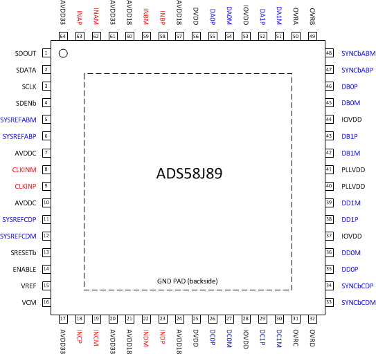
Pin Functions
| PIN | I/O | DESCRIPTION | |
|---|---|---|---|
| NAME | NO. | ||
| INPUT OR REFERENCE | |||
| INAP, INAM | 63, 62 | I | Differential analog input for channel A |
| INBP, INBM | 58, 59 | I | Differential analog input for channel B |
| INCP, INCM | 18, 19 | I | Differential analog input for channel C |
| INDP, INDM | 23, 22 | I | Differential analog input for channel D |
| VCM | 16 | O | Common mode output voltage to bias analog inputs, Vcm = 2.0 V |
| VREF | 15 | O | Voltage reference output. A 0.1-µF bypass capacitor to ground close to the pin is recommended |
| CLOCK/SYNC | |||
| CLKINP, CLKINM | 9, 8 | I | Differential clock input for channel |
| SYSREFABP, SYSREFABM | 6, 5 | I | LVDS input with internal 100-Ω termination. External SYSREF input for channels A, B, C, and D |
| SYSREFCDP, SYSREFCDM | 11, 12 | I | LVDS input with internal 100-Ω termination. External SYSREF input for channels C and D if output rate of channel A/B is different from channel C/D. Can be configured to trigger input for burst modes with SPI register write. Can be used as differential input or two single-ended inputs (SYSREFCDP becomes TRIGGERAB and SYSREFCDM becomes TRIGGERCD) for channel A/B and channel C/D. |
| CONTROL OR SERIAL | |||
| ENABLE | 14 | I | Chip enable. Active high. Power down functionality can be configured through SPI register setting and exercised using the ENABLE pin. Internal 51-kΩ pulldown resistor. |
| SCLK | 3 | I | Serial interface clock input |
| SDATA | 2 | I/O | Bidirectional serial data in 3-pin mode. In 4-pin interface, the SDATA pin is an input only. |
| SDENb | 4 | I | Serial interface enable |
| SDOUT | 1 | O | Serial interface data output |
| SRESETb | 13 | I | Hardware reset. Active low. Initializes internal registers during high to low transition. This pin has an internal 51-kΩ pullup resistor. |
| DATA OUTPUT INTERFACE | |||
| DA[0,1]P, DA[0,1]M | 55, 54, 52, 51 | O | JESD204B output interface for channel A |
| DB[0,1]P, DB[0,1]M | 46, 45, 43, 42 | O | JESD204B output interface for channel B |
| DC[0,1]P, DC[0,1]M | 26, 27, 29, 30 | O | JESD204B output interface for channel C |
| DD[0,1]P, DD[0,1]M | 35, 36, 38, 39 | O | JESD204B output interface for channel D |
| OVRA | 50 | I/O | Fast over-range indicator channel A. In burst mode can be configured to TRIGGERAB input. |
| OVRB | 49 | O | Fast over-range indicator channel B. In burst mode can be configured to TRDY output. |
| OVRC | 31 | I/O | Fast over-range indicator channel C. In burst mode can be configured to TRIGGERCD input. |
| OVRD | 32 | O | Fast over-range indicator channel D. In burst mode can be configured to TRDY output. |
| SYNCbABP, SYNCbABM | 47, 48 | I | SYNCb input for JESD204B interface for channel A/B, internal 100-Ω termination |
| SYNCbCDP, SYNCbCDM | 34, 33 | I | SYNCb input for JESD204B interface for channel C/D, internal 100-Ω termination |
| POWER SUPPLY | |||
| AVDDC | 7, 10 | I | Clock 1.8-V power supply |
| AVDD18 | 21, 24, 57, 60 | I | Analog 1.9-V power supply |
| AVDD33 | 17, 20, 61, 64 | I | Analog 3.3-V power supply |
| DVDD | 25, 56 | I | Digital 1.8-V power supply |
| GND | PowerPAD™ | I | Ground |
| IOVDD | 28, 37, 44, 53 | I | JESD204B output interface 1.8-V power supply |
| PLLVDD | 40, 41 | I | PLL 1.8-V power supply |