SBAS587A January 2014 – April 2014 ADS7251 , ADS7851
PRODUCTION DATA.
- 1 Features
- 2 Applications
- 3 Description
- 4 Revision History
- 5 Terminal Configuration and Functions
-
6 Specifications
- 6.1 Absolute Maximum Ratings
- 6.2 Handling Ratings
- 6.3 Recommended Operating Conditions
- 6.4 Thermal Information
- 6.5 Electrical Characteristics: ADS7251
- 6.6 Electrical Characteristics: ADS7851
- 6.7 Electrical Characteristics: Common
- 6.8 ADS7251 Timing Characteristics
- 6.9 ADS7851 Timing Characteristics
- 6.10 Typical Characteristics: ADS7251
- 6.11 Typical Characteristics: ADS7851
- 6.12 Typical Characteristics: Common
- 7 Detailed Description
- 8 Application and Implementation
- 9 Power Supply Recommendations
- 10Layout
- 11Device and Documentation Support
- 12Mechanical, Packaging, and Orderable Information
Package Options
Mechanical Data (Package|Pins)
- RTE|16
Thermal pad, mechanical data (Package|Pins)
- RTE|16
Orderable Information
8 Application and Implementation
8.1 Application Information
The two primary circuits required to maximize the performance of a high-precision, successive approximation register (SAR), analog-to-digital converter (ADC) are the input driver and the reference driver circuits. The ADS7851 and ADS7251 feature an internal reference designed to support device requirements. This section details some general principles for designing the input driver circuit and provides some application circuits designed using these devices.
8.2 Typical Application
The application circuit shown in Figure 44 is optimized for using the ADS7251 at a 2-MSPS throughput to achieve lowest distortion and lowest noise for input signal frequencies up to 100 kHz.
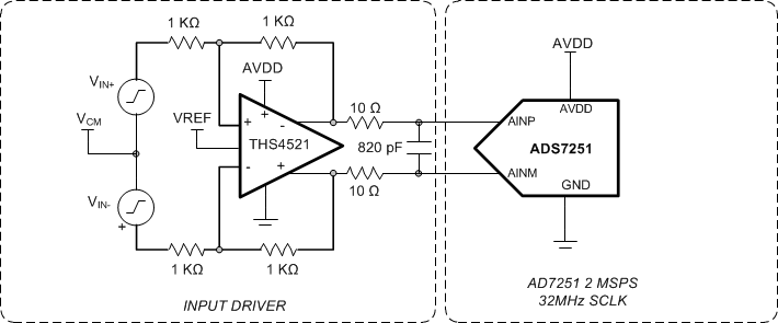 Figure 44. ADS7251 DAQ Circuit: Maximum SINAD for Input Signal Frequencies up to 100 kHz
The application circuit shown in Figure 45 is optimized for using the ADS7851 at a 1.5-MSPS throughput to achieve lowest distortion and lowest noise for input signal frequencies up to 100 kHz.
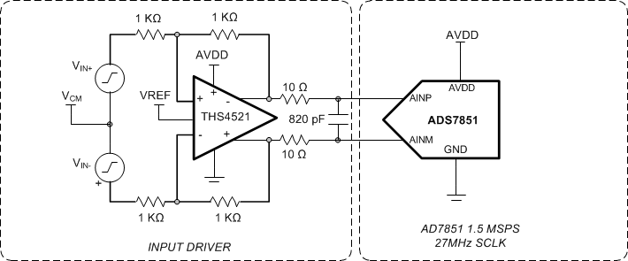 Figure 45. ADS7851 DAQ Circuit: Maximum SINAD for Input Signal Frequencies up to 100 kHz
8.2.1 Design Requirements
For the ADS7251, design an input driver and reference driver circuit to achieve > 71-dB SNR and < –90-dB THD at input frequencies of 10 kHz and 100 kHz.
For the ADS7851, design an input driver and reference driver circuit to achieve > 81-dB SNR and < –90-dB THD at input frequencies of 10 kHz and 100 kHz.
8.2.2 Detailed Design Procedure
The input driver circuit for a high-precision ADC mainly consists of two parts: a driving amplifier and an antialiasing filter. Careful design of the front-end circuit is critical to meet the linearity and noise performance of a high-precision ADC.
8.2.2.1 Input Amplifier Selection
Selection criteria for the input amplifiers is highly dependent on the input signal type and the performance goals of the data acquisition system. Some key amplifier specifications to consider while selecting an appropriate amplifier to drive the inputs of the ADC are:
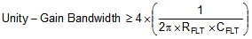
- Small-signal bandwidth. Select the small-signal bandwidth of the input amplifiers to be as high as possible after meeting the power budget of the system. Higher bandwidth reduces the closed-loop output impedance of the amplifier, thus allowing the amplifier to more easily drive the low cutoff frequency RC filter at the ADC inputs. Higher bandwidth also minimizes the harmonic distortion at higher input frequencies. In order to maintain the overall stability of the input driver circuit, the amplifier bandwidth should be selected as described in Equation 9:
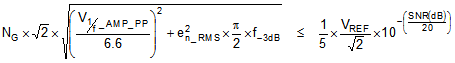
- Noise. Noise contribution of the front-end amplifiers should be as low as possible to prevent any degradation in SNR performance of the system. As a rule of thumb, to ensure that the noise performance of the data acquisition system is not limited by the front-end circuit, the total noise contribution from the front-end circuit should be kept below 20% of the input-referred noise of the ADC. Noise from the input driver circuit is bandlimited by designing a low cutoff frequency RC filter, as explained in Equation 10.
- V1 / f_AMP_PP is the peak-to-peak flicker noise in µVRMS,
- en_RMS is the amplifier broadband noise density in nV/√Hz,
- f–3dB is the 3-dB bandwidth of the RC filter, and
- NG is the noise gain of the front-end circuit, which is equal to '1' in a buffer configuration.
- Distortion. Both the ADC and the input driver introduce nonlinearity in a data acquisition block. As a rule of thumb, to ensure that the distortion performance of the data acquisition system is not limited by the front-end circuit, the distortion of the input driver should be at least 10 dB lower than the distortion of the ADC, as shown in Equation 11.
- Settling Time. For dc signals with fast transients that are common in a multiplexed application, the input signal must settle to the desired accuracy at the inputs of the ADC during the acquisition time window. This condition is critical to maintain the overall linearity performance of the ADC. Typically, the amplifier data sheets specify the output settling performance only up to 0.1% to 0.001%, which may not be sufficient for the desired accuracy. Therefore, the settling behavior of the input driver should always be verified by TINA™-SPICE simulations before selecting the amplifier.
where:

The distortion resulting from variation in the common-mode signal is eliminated by using a fully-differential amplifier (FDA) in an inverting gain configuration that establishes a fixed common-mode level at the ADC input. This configuration also eliminates the requirement of rail-to-rail swing at the amplifier input. The low-power THS4521, used as an input driver, provides exceptional ac performance because of its extremely low-distortion and high-bandwidth specifications. The device REFOUT_x pin can be directly connected to the VOCM pin of the THS4521 to set the output common-mode voltage to 2.5 V, as required by the ADC.
8.2.2.2 Antialiasing Filter
Converting analog-to-digital signals requires sampling an input signal at a constant rate. Any higher frequency content in the input signal beyond half the sampling frequency is digitized and folded back into the low-frequency spectrum. This process is called aliasing. Therefore, an analog, antialiasing filter must be used to remove the harmonic content from the input signal before being sampled by the ADC. An antialiasing filter is designed as a low-pass, RC filter, for which the 3-dB bandwidth is optimized based on specific application requirements (as shown in Figure 46). For dc signals with fast transients (including multiplexed input signals), a high-bandwidth filter is designed to allow accurately settling the signal at the ADC inputs during the small acquisition time window. For ac signals, the filter bandwidth should be kept low to band-limit the noise fed into the ADC input, thereby increasing the signal-to-noise ratio (SNR) of the system.
Besides filtering the noise from the front-end drive circuitry, the RC filter also helps attenuate the sampling charge injection from the switched-capacitor input stage of the ADC. A filter capacitor, CFLT, is connected across the ADC inputs. This capacitor helps reduce the sampling charge injection and provides a charge bucket to quickly charge the internal sample-and-hold capacitors during the acquisition process. As a rule of thumb, the value of this capacitor should be at least 10 times the specified value of the ADC sampling capacitance. For these devices, the input sampling capacitance is equal to 40 pF. Thus, the value of CFLT should be greater than 400 pF. The capacitor should be a COG- or NPO-type because these capacitor types have a high-Q, low-temperature coefficient, and stable electrical characteristics under varying voltages, frequency, and time.
Note that driving capacitive loads can degrade the phase margin of the input amplifiers, thus making the amplifier marginally unstable. To avoid amplifier stability issues, series isolation resistors (RFLT) are used at the output of the amplifiers. A higher value of RFLT is helpful from the amplifier stability perspective, but adds distortion as a result of interactions with the nonlinear input impedance of the ADC. Distortion increases with source impedance, input signal frequency, and input signal amplitude. Therefore, the selection of RFLT requires balancing the stability and distortion of the design. For these devices, TI recommends limiting the value of RFLT to a maximum of 22 Ω in order to avoid any significant degradation in linearity performance. The tolerance of the selected resistors can be chosen as 1% because the use of a differential capacitor at the input balances the effects resulting from any resistor mismatch.
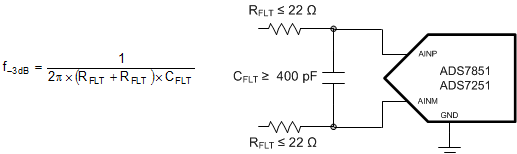 Figure 46. Antialiasing Filter
The input amplifier bandwidth should be much higher than the cutoff frequency of the antialiasing filter. TI strongly recommends performing a SPICE simulation to confirm that the amplifier has more than 40° phase margin with the selected filter. Simulation is critical because even with high-bandwidth amplifiers, some amplifiers might require more bandwidth than others to drive similar filters. If an amplifier has less than a 40° phase margin with 22-Ω resistors, using a different amplifier with higher bandwidth or reducing the filter cutoff frequency with a larger differential capacitor is advisable.
In addition, the components of the antialiasing filter are such that the noise from the front-end circuit is kept low without adding distortion to the input signal.
8.2.3 Application Curves
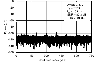
Figure 47 shows an FFT plot for the ADS7251 with the circuit shown in Figure 44 and an input frequency of
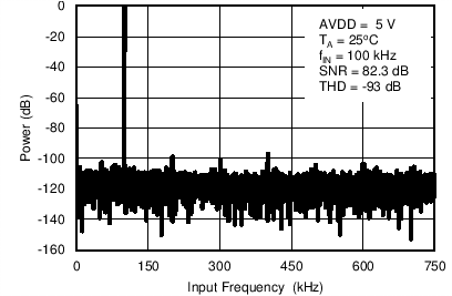
10 kHz. Figure 48 shows an FFT plot for the ADS7251 with the same circuit configuration but for an input frequency of 100 kHz.
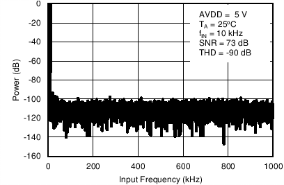
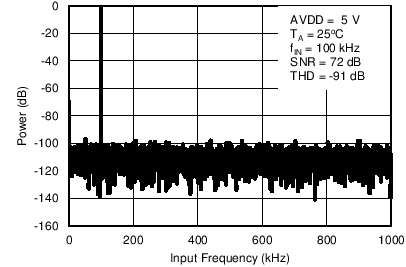
Figure 49 shows an FFT plot for the ADS7851 with the circuit shown in Figure 45 and an input frequency of
10 kHz. Figure 50 shows an FFT plot for the ADS7251 with the same circuit configuration but for an input frequency of 100 kHz.