SBAS587A January 2014 – April 2014 ADS7251 , ADS7851
PRODUCTION DATA.
- 1 Features
- 2 Applications
- 3 Description
- 4 Revision History
- 5 Terminal Configuration and Functions
-
6 Specifications
- 6.1 Absolute Maximum Ratings
- 6.2 Handling Ratings
- 6.3 Recommended Operating Conditions
- 6.4 Thermal Information
- 6.5 Electrical Characteristics: ADS7251
- 6.6 Electrical Characteristics: ADS7851
- 6.7 Electrical Characteristics: Common
- 6.8 ADS7251 Timing Characteristics
- 6.9 ADS7851 Timing Characteristics
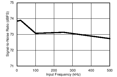
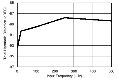
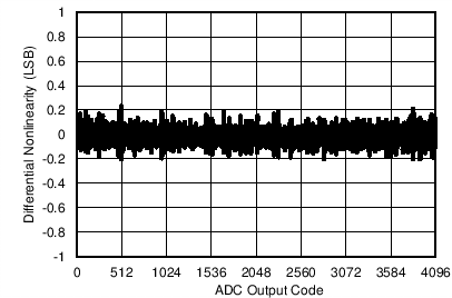
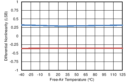
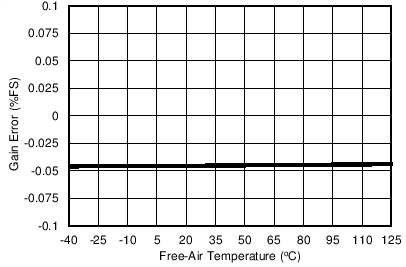
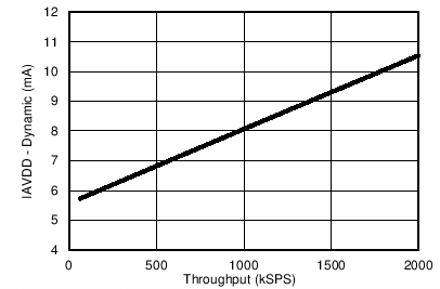
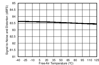
- 6.10 Typical Characteristics: ADS7251
- 6.11 Typical Characteristics: ADS7851
- 6.12 Typical Characteristics: Common
- 7 Detailed Description
- 8 Application and Implementation
- 9 Power Supply Recommendations
- 10Layout
- 11Device and Documentation Support
- 12Mechanical, Packaging, and Orderable Information
Package Options
Mechanical Data (Package|Pins)
- RTE|16
Thermal pad, mechanical data (Package|Pins)
- RTE|16
Orderable Information
6 Specifications
6.1 Absolute Maximum Ratings(1)
over operating free-air temperature range (unless otherwise noted)| MIN | MAX | UNIT | ||
|---|---|---|---|---|
| Supply voltage | AVDD to GND | –0.3 | +7 | V |
| DVDD to GND | –0.3 | +7 | V | |
| Analog input voltage | AINP_x to REFGND_x | REFGND_x – 0.3 | AVDD + 0.3 | V |
| AINM_x to REFGND_x | REFGND_x – 0.3 | AVDD + 0.3 | V | |
| Digital input voltage | CS, SCLK to GND | GND – 0.3 | DVDD + 0.3 | V |
| Ground voltage difference | | REFGND_x – GND | | 0.3 | V | |
| Input current | Any pin except supply pins | ±10 | mA | |
| Maximum virtual junction temperature, TJ | +150 | °C | ||
(1) Stresses beyond those listed under Absolute Maximum Ratings may cause permanent damage to the device. These are stress ratings only, which do not imply functional operation of the device at these or any other conditions beyond those indicated under Recommended Operating Conditions. Exposure to absolute-maximum-rated conditions for extended periods may affect device reliability.
6.2 Handling Ratings
| MIN | MAX | UNIT | ||
|---|---|---|---|---|
| Tstg | Storage temperature range | –65 | +150 | °C |
| VESD(1), all pins |
Human body model (HBM) ESD stress voltage(2), JEDEC standard 22, test method A114-C.01 |
±2000 | V | |
| Charged device model (CDM) ESD stress voltage(3), JEDEC standard 22, test method C101 |
±500 | V |
(1) Electrostatic discharge (ESD) to measure device sensitivity and immunity to damage caused by assembly line electrostatic discharges in to the device.
(2) Level listed above is the passing level per ANSI, ESDA, and JEDEC JS-001. JEDEC document JEP155 states that ±2000-V HBM allows safe manufacturing with a standard ESD control process.
(3) Level listed above is the passing level per EIA-JEDEC JESD22-C101. JEDEC document JEP157 states that ±500-V CDM allows safe manufacturing with a standard ESD control process.
6.3 Recommended Operating Conditions
over operating free-air temperature range (unless otherwise noted)| MIN | NOM | MAX | UNIT | ||
|---|---|---|---|---|---|
| AVDD | Analog supply voltage | 5 | V | ||
| DVDD | Digital supply voltage | 3.3 | V | ||
6.4 Thermal Information
| THERMAL METRIC(1) | ADS7251, ADS7851 | UNIT | |
|---|---|---|---|
| RTE (WQFN) | |||
| 16 TERMINALS | |||
| RθJA | Junction-to-ambient thermal resistance | 33.3 | °C/W |
| RθJC(top) | Junction-to-case (top) thermal resistance | 29.5 | |
| RθJB | Junction-to-board thermal resistance | 7.3 | |
| ψJT | Junction-to-top characterization parameter | 0.2 | |
| ψJB | Junction-to-board characterization parameter | 7.4 | |
| RθJC(bot) | Junction-to-case (bottom) thermal resistance | 0.9 | |
(1) For more information about traditional and new thermal metrics, see the IC Package Thermal Metrics application report, SPRA953.
6.5 Electrical Characteristics: ADS7251
All minimum and maximum specifications are at TA = –40°C to +125°C, AVDD = 5 V, VREF_A = VREF_B = 2.5 V, and fDATA =2 MSPS, unless otherwise noted. Typical values are at TA = +25°C, AVDD = 5 V, and DVDD = 3.3 V.
6.6 Electrical Characteristics: ADS7851
All minimum and maximum specifications are at TA = –40°C to +125°C, AVDD = 5 V, VREF_A = VREF_B = 2.5 V, and fDATA =1.5 MSPS, unless otherwise noted. Typical values are at TA = +25°C, AVDD = 5 V, and DVDD = 3.3 V.
6.7 Electrical Characteristics: Common
All minimum and maximum specifications are at TA = –40°C to +125°C, AVDD = 5 V, VREF_A = VREF_B = 2.5 V, and fDATA =2 MSPS, unless otherwise noted. Typical values are at TA = +25°C, AVDD = 5 V, and DVDD = 3.3 V.
| PARAMETER | TEST CONDITIONS | MIN | TYP | MAX | UNIT | ||
|---|---|---|---|---|---|---|---|
| ANALOG INPUT | |||||||
| FSR | Full-scale input range (AINP_x – AINM_x) |
For AVDD ≥ 5 V | –2 VREF | 2 VREF | V | ||
| For AVDD < 5 V | –AVDD | AVDD | V | ||||
| VIN | Absolute input voltage (AINP_x or AIM_x to REFGND_x) |
For AVDD ≥ 5 V | 0 | 2 VREF | V | ||
| For AVDD < 5 V | 0 | AVDD | V | ||||
| VCM | Input common-mode voltage range | VREF_A = VREF_B = VREF | VREF – 0.1 | VREF | VREF + 0.1 | V | |
| CIN | Input capacitance | In sample mode | 40 | pF | |||
| In hold mode | 4 | pF | |||||
| SAMPLING DYNAMICS | |||||||
| tA | Aperture delay | 8 | ns | ||||
| tA match | ADC_A to ADC_B | 40 | ps | ||||
| BW | Full-power bandwidth | At 3 dB | 25 | MHz | |||
| At 0.1 dB | 5 | MHz | |||||
| INTERNAL VOLTAGE REFERENCE | |||||||
| VREFOUT | Internal reference output voltage | At +25°C | 2.495 | 2.500 | 2.505 | V | |
| VREFOUT-match | VREFOUT matching | | REFOUT_A – REFOUT_B | | ±1 | mV | |||
| dVREFOUT/dt | Long-term voltage drift | 1000 hours | 150 | ppm | |||
| dVREFOUT/dT | Reference voltage drift with temperature | ±10 | ppm/°C | ||||
| RO | Internal reference output impedance | 1 | Ω | ||||
| COUT | External output capacitor | 22 | μF | ||||
| Internal reference output settling time | COUT = 22 μF | 10 | ms | ||||
| DIGITAL INPUTS(1) | |||||||
| VIH | Input voltage, high | 0.7 DVDD | DVDD + 0.3 | V | |||
| VIL | Input voltage, low | –0.3 | 0.3 DVDD | V | |||
| CIN | Input capacitance | 5 | pF | ||||
| IIN | Input leakage current | 0 ≤ Vdigital-input ≤ DVDD | ±0.1 | 1 | μA | ||
| DIGITAL OUTPUTS(1) | |||||||
| VOH | Output voltage, high | IOH = 500-µA source | 0.8 DVDD | DVDD | V | ||
| VOL | Output voltage, low | IOH = 500-µA sink | 0 | 0.2 DVDD | V | ||
| POWER SUPPLY | |||||||
| AVDD | Supply voltage | Analog (AVDD to GND) | 4.75(2) | 5.0 | 5.25 | V | |
| DVDD | Digital (DVDD to GND) | Operational range | 1.65 | 3.3 | 5.25 | V | |
| For specified performance | 1.65 | 3 | 3.6 | V | |||
| TEMPERATURE RANGE | |||||||
| TA | Operating free-air temperature | –40 | +125 | °C | |||
(1) Specified by design; not production tested.
(2) The AVDD supply voltage defines the permissible voltage swing on the analog input pins. Refer to the Power Supply Recommendations section for more details.
6.8 ADS7251 Timing Characteristics
| PARAMETER | TEST CONDITIONS | MIN | TYP | MAX | UNIT | ||
|---|---|---|---|---|---|---|---|
| fTHROUGHPUT | Throughput | fCLK = max | 2000 | kSPS | |||
| fCLK | CLOCK frequency | fTHROUGHPUT = max | 32 | MHz | |||
| tCLK | CLOCK period | fTHROUGHPUT = max | 31.25 | ns | |||
| tPH_CK | CLOCK high time | 0.45 | 0.55 | tCLK | |||
| tPL_CK | CLOCK low time | 0.45 | 0.55 | tCLK | |||
| tCONV | Conversion time | tSU_CSCK + 12 tCLK | ns | ||||
| tACQ | Acquisition time | fCLK = max | 75 | ns | |||
| tPH_CS | CS high time | 30 | ns | ||||
| tD_CKDO | Delay time | SCLK rising edge to (next) data valid | 15 | ns | |||
| tDV_CSDO | CS falling to data enable | 10 | ns | ||||
| tD_CKCS | Last SCLK rising to CS rising | 5 | ns | ||||
| tDZ_CSDO | CS rising to DOUT going to 3-state | 10 | ns | ||||
| tSU_CSCK | Setup time | CS falling to SCLK falling | 15 | ns | |||
Figure 1 shows the details of the serial interface between the ADS7251 and the digital host controller.
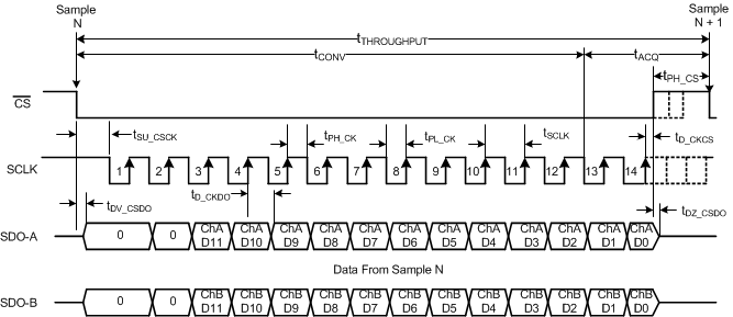 Figure 1. ADS7251 Serial Interface Timing Diagram
6.9 ADS7851 Timing Characteristics
| PARAMETER | TEST CONDITIONS | MIN | TYP | MAX | UNIT | ||
|---|---|---|---|---|---|---|---|
| fTHROUGHPUT | Sample taken to data read | fCLK = max | 1500 | kSPS | |||
| fCLK | CLOCK frequency | fTHROUGHPUT = max | 27 | MHz | |||
| tCLK | CLOCK period | fTHROUGHPUT = max | 37 | ns | |||
| tPH_CK | CLOCK high time | 0.45 | 0.55 | tCLK | |||
| tPL_CK | CLOCK low time | 0.45 | 0.55 | tCLK | |||
| tCONV | Conversion time | tSU_CSCK + 14 tCLK | ns | ||||
| tACQ | Acquisition time | fCLK = max | 90 | ns | |||
| tPH_CS | CS high time | 30 | ns | ||||
| tD_CKDO | Delay time | SCLK rising edge to (next) data valid | 15 | ns | |||
| tDV_CSDO | CS falling to data enable | 10 | ns | ||||
| tD_CKCS | Last SCLK rising to CS rising | 5 | ns | ||||
| tDZ_CSDO | CS rising to DOUT going to 3-state | 10 | ns | ||||
| tSU_CSCK | Setup time | CS falling to SCLK falling | 15 | ns | |||
Figure 2 shows the details of the serial interface between the ADS7851 and the digital host controller.
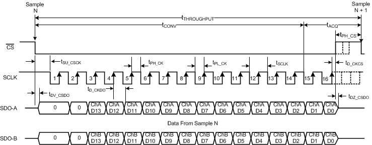 Figure 2. ADS7851 Serial Interface Timing Diagram
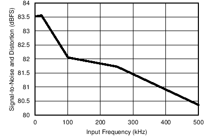
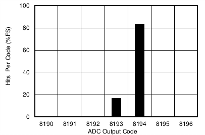
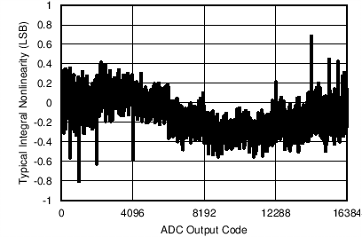
6.10 Typical Characteristics: ADS7251
At TA = +25°C, AVDD = 5 V, DVDD = 3.3 V, VREF = 2.5 V (internal), and fDATA = 1 MSPS, unless otherwise noted.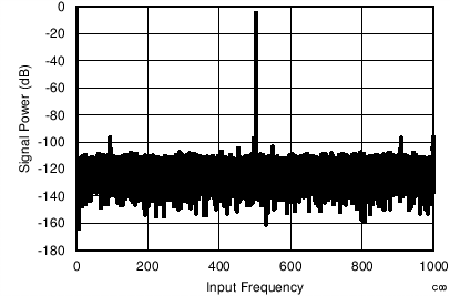
| fIN = 500 kHz | ||
| fIN = 10 kHz | ||
| fIN = 10 kHz | ||
| fIN = 10 kHz | ||
| fIN = 10 kHz | ||
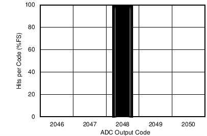
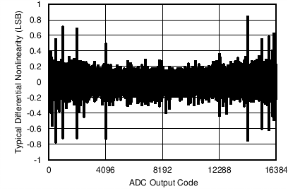
| VIN-DIFF = 0 V | 65536 Data Points | |
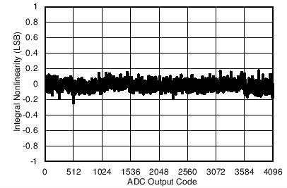
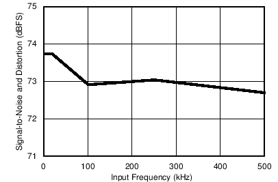
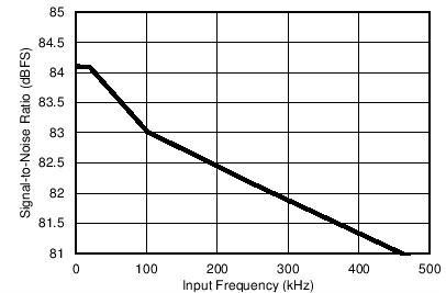
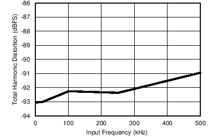
6.11 Typical Characteristics: ADS7851
At TA = +25°C, AVDD = 5 V, DVDD = 3.3 V, VREF = 2.5 V (internal), and fDATA = 1 MSPS, unless otherwise noted.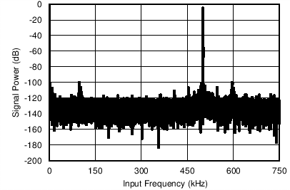
| fIN = 500 kHz | ||
| fIN = 10 kHz | ||
| fIN = 10 kHz | ||
| fIN = 10 kHz | ||
| fIN = 10 kHz | ||
| VIN-DIFF = 0 V | 65536 Data Points | |
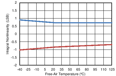
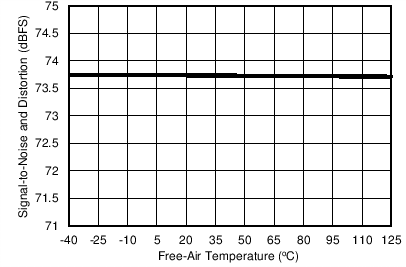
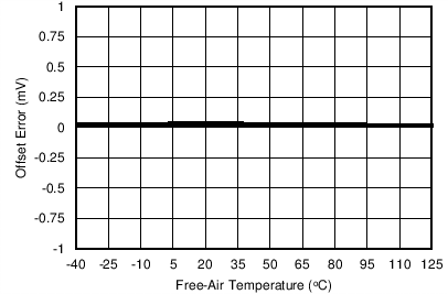
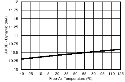
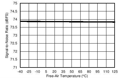
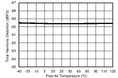
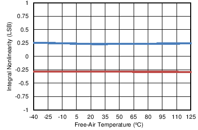
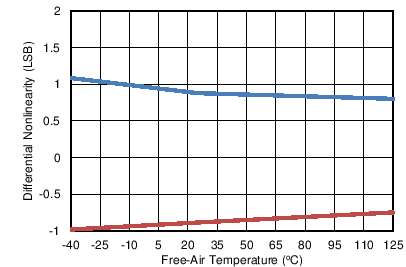
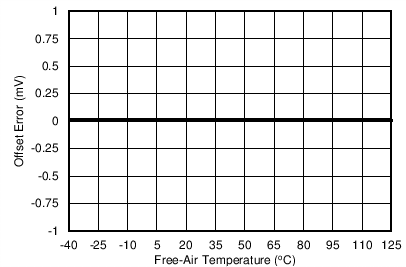
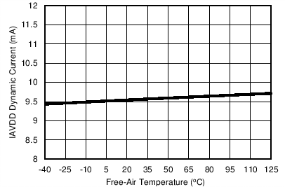
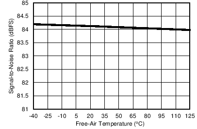
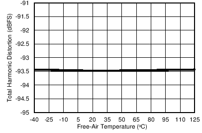
6.12 Typical Characteristics: Common
At TA = +25°C, AVDD = 5 V, DVDD = 3.3 V, and VREF = 2.5 V (internal), unless otherwise noted.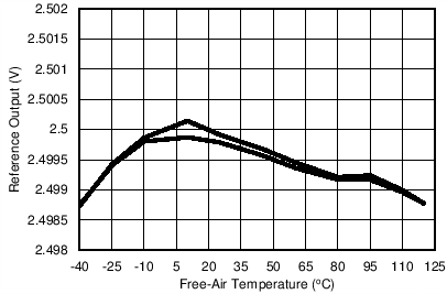
Device Temperature
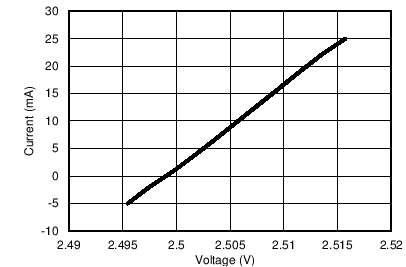
| Rout = 0.75 Ω Typ | ||
Output Current vs Output Voltage