SBAS587A January 2014 – April 2014 ADS7251 , ADS7851
PRODUCTION DATA.
- 1 Features
- 2 Applications
- 3 Description
- 4 Revision History
- 5 Terminal Configuration and Functions
-
6 Specifications
- 6.1 Absolute Maximum Ratings
- 6.2 Handling Ratings
- 6.3 Recommended Operating Conditions
- 6.4 Thermal Information
- 6.5 Electrical Characteristics: ADS7251
- 6.6 Electrical Characteristics: ADS7851
- 6.7 Electrical Characteristics: Common
- 6.8 ADS7251 Timing Characteristics
- 6.9 ADS7851 Timing Characteristics
- 6.10 Typical Characteristics: ADS7251
- 6.11 Typical Characteristics: ADS7851
- 6.12 Typical Characteristics: Common
- 7 Detailed Description
- 8 Application and Implementation
- 9 Power Supply Recommendations
- 10Layout
- 11Device and Documentation Support
- 12Mechanical, Packaging, and Orderable Information
Package Options
Mechanical Data (Package|Pins)
- RTE|16
Thermal pad, mechanical data (Package|Pins)
- RTE|16
Orderable Information
7 Detailed Description
7.1 Overview
The ADS7251 and ADS7851 are pin-compatible, dual, simultaneous-sampling, analog-to-digital converters (ADCs). Each device features two independent internal voltage references and supports fully-differential input signals with the input common-mode on each input pin equal to the reference voltage. The full-scale input signal on each input pin is equal to twice the reference voltage. The devices provide a simple, serial interface to the host controller and operate over a wide range of digital power supplies.
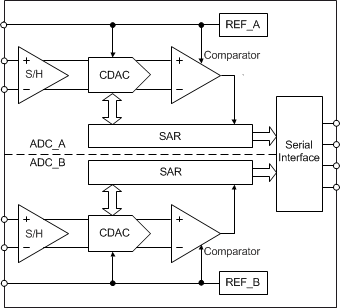
7.2 Functional Block Diagram
7.3 Feature Description
7.3.1 Reference
The device has two simultaneous sampling ADCs (ADC_A and ADC_B) and two independent internal reference sources (INTREF_A and INTREF_B). INTREF_A outputs voltage VREF_A on pin REFOUT_A and INTREF_B outputs voltage VREF_B on pin REFOUT_B. As shown in Figure 38, the REFOUT_A and REFOUT_B pins must be decoupled with the REFGND_A and REFGND_B pins, respectively, with individual 22-µF decoupling capacitors. ADC_A operates with reference voltage VREF_A and ADC_B operates with reference voltage VREF_B.
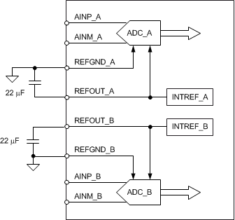 Figure 38. Reference Block Diagram
7.3.2 Analog Input
The devices support fully-differential analog input signals. These inputs are sampled and converted simultaneously by the two ADCs, ADC_A and ADC_B. Figure 39a and Figure 39b show equivalent circuits for the ADC_A and ADC_B analog input pins, respectively.
Series resistance (RS) represents the on-state sampling switch resistance (typically 50 Ω) and CSAMPLE is the device sampling capacitor (typically 40 pF). ADC_A samples VAINP_A and VAINM_A and converts for the difference voltage (VAINP_A – VAINM_A). ADC_B samples VAINP_B and VAINM_B and converts for the difference voltage (VAINP_B – VAINM_B).
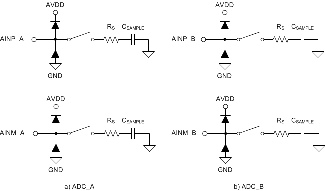 Figure 39. Equivalent Circuit for the Analog Input Pins
7.3.2.1 Analog Input Full-Scale Range
The analog input full-scale range (FSR) for ADC_A and ADC_B is twice the reference voltage provided to the particular ADC. Therefore, the FSR for ADC_A and ADC_B can be determined by Equation 1 and Equation 2, respectively:
To use the full dynamic input range on the analog input pins, AVDD must be as shown in Equation 3, Equation 4, and Equation 5:
7.3.2.2 Common-Mode Voltage Range
For the analog input, the devices support a common-mode voltage equal to the reference voltage provided to the ADC. Therefore, the common-mode voltage for the ADC_A and ADC_B must be as shown in Equation 6 and Equation 7, respectively.
7.3.3 ADC Transfer Function
The device output is in twos compliment format. Device resolution for the fully-differential input can be computed by Equation 8:
where:
Table 1 shows the different input voltages and the corresponding device output codes. Figure 40 shows the ideal transfer characteristics for the device.
Table 1. Transfer Characteristics
| INPUT VOLTAGE (AINP_x – AINM_x) |
OUTPUT CODE (Hex) | ||
|---|---|---|---|
| CODE | ADS7251 | ADS7851 | |
| < –2 × VREF | NFSC | 800 | 2000 |
| –2 × VREF + 1 LSB | NFSC + 1 | 801 | 2001 |
| –1 LSB | MC | FFF | 3FFF |
| 0 | PLC | 000 | 0000 |
| > 2 × VREF – 1 LSB | PFSC | 7FF | 1FFF |
 Figure 40. Ideal Transfer Characteristics
7.4 Device Functional Modes
7.4.1 Serial Interface
The devices support a simple, SPI-compatible interface to the external digital host. The CS signal defines one conversion and serial transfer frame. A frame starts with a CS falling edge and ends with a CS rising edge. The SDO_A and SDO_B pins output the ADC_A and ADC_B conversion results, respectively. Figure 41 shows a detailed timing diagram for the ADS7251.
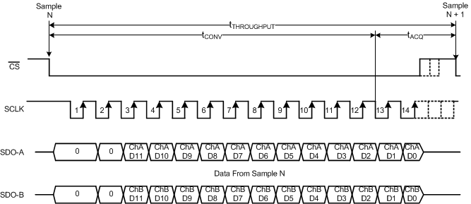 Figure 41. ADS7251 Serial Interface Timing Diagram
Figure 42 shows a detailed timing diagram for the ADS7851.
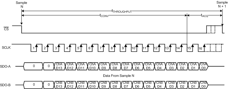 Figure 42. ADS7851 Serial Interface Timing Diagram
A CS falling edge brings the serial data bus out of 3-state and also outputs '0' on the SDO_A and SDO_B pins. A minimum delay of tSU_CSCK must elapse between the CS falling edge and the first SCLK falling edge. The subsequent clock edges are used to shift out the conversion result using the serial interface, as shown in Table 2. The sample-and-hold circuit returns to sample mode as soon as the conversion process is over. Any extra clock edges output a '0' on the SDO pins. A CS rising edge ends the frame and brings the serial data bus to 3-state.
Table 2. Data Launch Edge
| DEVICE | PIN | LAUNCH EDGE | |||||||||
|---|---|---|---|---|---|---|---|---|---|---|---|
| CS↓ | SCLK | CS↑ | |||||||||
| ↓1 | ↓2 | … | ↓13 | ↓14 | ↓15 | ↓16 | … | ||||
| ADS7851 | SDO-A | 0 | 0 | D13_A | … | D2_A | D1_A | D0_A | 0 | … | Hi-Z |
| SDO-B | 0 | 0 | D13_B | … | D2_B | D1_B | D0_B | 0 | … | Hi-Z | |
| ADS7251 | SDO-A | 0 | 0 | D11_A | … | D0_A | 0 | 0 | 0 | … | Hi-Z |
| SDO-B | 0 | 0 | D11_B | … | D0_B | 0 | 0 | 0 | … | Hi-Z | |
7.4.2 Short-Cycling Feature
For the ADS7851, a minimum of 16 SCLK rising edges must be provided between the beginning and end of the frame to complete the 14-bit data transfer. For the ADS7251, a minimum of 14 SCLK rising edges must be provided between the beginning and end of the frame to complete the 12-bit data transfer. As shown in Figure 43, if CS is brought high before the expected number of SCLK rising edges are provided, the current frame is aborted and the device starts sampling the new analog input signal. However, the output data bits latched into the digital host before this CS rising edge are still valid data corresponding to sample N.
After aborting the current frame, CS must be kept high for tACQ to ensure minimum acquisition time is provided for the next conversion.
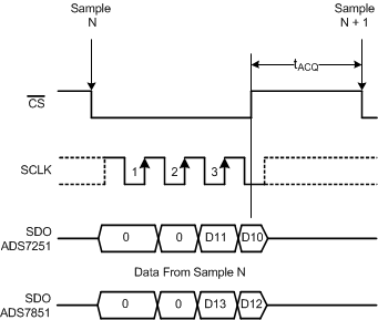 Figure 43. Short-Cycling Feature