SBAS761A February 2020 – February 2020 ADS8355
PRODUCTION DATA.
- 1 Features
- 2 Applications
- 3 Description
- 4 Revision History
- 5 Pin Configuration and Functions
- 6 Specifications
-
7 Detailed Description
- 7.1 Overview
- 7.2 Functional Block Diagram
- 7.3 Feature Description
- 7.4 Device Functional Modes
- 7.5 Programming
- 7.6
Register Map
- 7.6.1
ADS8355 Registers
- 7.6.1.1 PD_STANDBY Register (Offset = 4h) [reset = 0h]
- 7.6.1.2 PD_KEY Register (Offset = 5h) [reset = 0h]
- 7.6.1.3 SDO_CTRL Register (Offset = Dh) [reset = 0h]
- 7.6.1.4 DATA_OUT_CTRL Register (Offset = 11h) [reset = 0h]
- 7.6.1.5 REF_SEL Register (Offset = 20h) [reset = 0h]
- 7.6.1.6 REFDAC_A_LSB Register (Offset = 24h) [reset = 0h]
- 7.6.1.7 REFDAC_A_MSB Register (Offset = 25h) [reset = 0h]
- 7.6.1.8 REFDAC_B_LSB Register (Offset = 26h) [reset = 0h]
- 7.6.1.9 REFDAC_B_MSB Register (Offset = 27h) [reset = 0h]
- 7.6.1.10 INPUT_CONFIG Register (Offset = 28h) [reset = 0h]
- 7.6.1
ADS8355 Registers
- 8 Application and Implementation
- 9 Power Supply Recommendations
- 10Layout
- 11Device and Documentation Support
- 12Mechanical, Packaging, and Orderable Information
Package Options
Mechanical Data (Package|Pins)
- RTE|16
Thermal pad, mechanical data (Package|Pins)
- RTE|16
Orderable Information
7.4.1 Conversion Data Read: Dual-SDO Mode (Default)
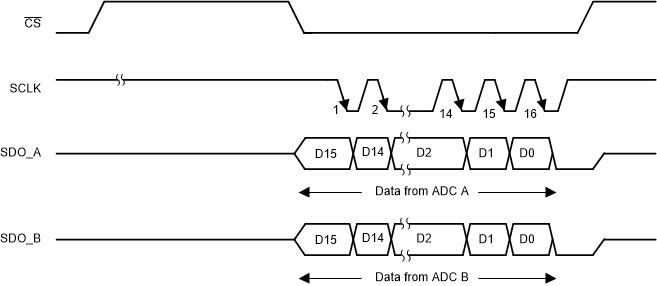
The dual-SDO mode is designed to support the maximum throughput at lower SCLK frequencies.
The single-SDO mode is enabled by programming the SDO_MODE bit in the SDO_CTRL register to logic low. In this mode, the SDO_A pin outputs the ADC_A conversion result and the SDO_B pin outputs the ADC_B conversion result. Figure 29 shows a detailed timing diagram for this mode.
 Figure 29. Dual-SDO Mode Timing Diagram
 A CS rising edge forces SDO_x to tri-state. CS also samples the input signal and causes the device to enter conversion phase. Conversion is done with the internal clock. CS and SCLK must remain high for a minimum time of tCONV. A CS falling edge brings the serial data bus out of tri-state and the device outputs the MSB of the data. The lower data bits are output on the subsequent SCLK falling edges. SDO_A and SDO_B go low after the 16th SCLK falling edge. The SDO_x signals remain low until the CS signal is pulled high.