SBAS905C November 2019 – July 2020 ADS8686S
PRODUCTION DATA
- 1 Features
- 2 Applications
- 3 Description
- 4 Revision History
- 5 Pin Configuration and Functions
-
6 Specifications
- 6.1 Absolute Maximum Ratings
- 6.2 ESD Ratings
- 6.3 Recommended Operating Conditions
- 6.4 Thermal Information
- 6.5 Electrical Characteristics
- 6.6 Timing Requirements
- 6.7 Switching Characteristics
- 6.8 Timing Diagrams: Universal
- 6.9 Timing Diagrams: Parallel Data Read
- 6.10 Timing Diagrams: Serial Data Read
- 6.11 Typical Characteristics
-
7 Detailed Description
- 7.1 Overview
- 7.2 Functional Block Diagram
- 7.3 Feature Description
- 7.4
Device Functional Modes
- 7.4.1
Device Interface: Pin Description
- 7.4.1.1 REFSEL (Input)
- 7.4.1.2 RESET (Input)
- 7.4.1.3 SEQEN (Input)
- 7.4.1.4 HW_RANGESEL[1:0] (Input)
- 7.4.1.5 SER/BYTE/PAR (Input)
- 7.4.1.6 DB[3:0] (Input/Output)
- 7.4.1.7 DB4/SER1W (Input/Output)
- 7.4.1.8 DB5/CRCEN (Input/Output)
- 7.4.1.9 DB[7:6] (Input/Output)
- 7.4.1.10 DB8 (Input/Output)
- 7.4.1.11 DB9/BYTESEL (Input/Output)
- 7.4.1.12 DB10/SDI (Input/Output)
- 7.4.1.13 DB11/SDOB (Input/Output)
- 7.4.1.14 DB12/SDOA (Input/Output)
- 7.4.1.15 DB13/OS0 (Input/Output)
- 7.4.1.16 DB14/OS1 (Input/Output)
- 7.4.1.17 DB15/OS2 (Input/Output)
- 7.4.1.18 WR/BURST (Input)
- 7.4.1.19 SCLK/RD (Input)
- 7.4.1.20 CS (Input)
- 7.4.1.21 CHSEL[2:0] (Input)
- 7.4.1.22 BUSY (Output)
- 7.4.1.23 CONVST (Input)
- 7.4.2 Device Modes of Operation
- 7.4.1
Device Interface: Pin Description
- 7.5 Programming
- 7.6 Register Maps
- 8 Application and Implementation
- 9 Power Supply Recommendations
- 10Layout
- 11Device and Documentation Support
Package Options
Mechanical Data (Package|Pins)
- PZA|80
Thermal pad, mechanical data (Package|Pins)
Orderable Information
7.4.2.4.1 Hardware Mode Channel Selection
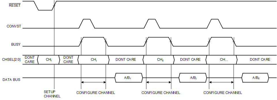
In hardware mode, the logic level of the CHSELx signals during an ongoing conversion determine the channel pair for next conversion. Table 7-7 lists the CHSELx signal decoding information. After a full or partial reset, the CHSELx signal status at the rising edge of the reset signal determines the initial channel pair to sample and convert when the first CONVST signal is available. Set the CHSELx signals to the required channel before CONVST goes from low to high and maintain the status until BUSY goes from high to low, indicating the conversion complete. The device samples the CHSELx status during conversion to select the channel pair for the next conversion. The multiplexer then establishes a relevant connection between the ADC driver of the selected channel and SAR ADC. Figure 7-12 shows a timing diagram of how this mode is selected.
| CHANNEL SELECTION INPUT PIN | ANALOG INPUT CHANNELS FOR CONVERSION | ||
|---|---|---|---|
| CHSEL2 | CHSEL1 | CHSEL0 | |
| 0 | 0 | 0 | AIN_0A, AIN_0B |
| 0 | 0 | 1 | AIN_1A, AIN_1B |
| 0 | 1 | 0 | AIN_2A, AIN_2B |
| 0 | 1 | 1 | AIN_3A, AIN_3B |
| 1 | 0 | 0 | AIN_4A, AIN_4B |
| 1 | 0 | 1 | AIN_5A, AIN_5B |
| 1 | 1 | 0 | AIN_6A, AIN_6B |
| 1 | 1 | 1 | AIN_7A, AIN_7B |
 Figure 7-12 Hardware Mode Channel Conversion Setting