SBAS547D May 2013 – August 2015 ADS8881
PRODUCTION DATA.
- 1 Features
- 2 Applications
- 3 Description
- 4 Revision History
- 5 Companion Products
- 6 Device Comparison
- 7 Pin Configurations and Functions
- 8 Specifications
- 9 Parametric Measurement Information
- 10Detailed Description
-
11Application and Implementation
- 11.1 Application Information
- 11.2 Typical Applications
- 12Power-Supply Recommendations
- 13Layout
- 14Device and Documentation Support
- 15Mechanical, Packaging, and Orderable Information
Package Options
Mechanical Data (Package|Pins)
Thermal pad, mechanical data (Package|Pins)
- DRC|10
Orderable Information
8 Specifications
8.1 Absolute Maximum Ratings
over operating free-air temperature range (unless otherwise noted)(1)| MIN | MAX | UNIT | ||
|---|---|---|---|---|
| AINP to GND or AINN to GND | –0.3 | REF + 0.3 | V | |
| AVDD to GND or DVDD to GND | –0.3 | 4 | V | |
| REF to GND | –0.3 | 5.7 | V | |
| Digital input voltage to GND | –0.3 | DVDD + 0.3 | V | |
| Digital output to GND | –0.3 | DVDD + 0.3 | V | |
| Operating temperature, TA | ADS8881C | 0 | 70 | °C |
| ADS8881I | –40 | 85 | ||
| Storage temperature, Tstg | –65 | 150 | °C | |
8.2 ESD Ratings
| VALUE | UNIT | |||
|---|---|---|---|---|
| V(ESD) | Electrostatic discharge | Human-body model (HBM), per ANSI/ESDA/JEDEC JS-001(1) | ±2000 | V |
| Charged-device model (CDM), per JEDEC specification JESD22-C101(2) | ±500 | |||
8.3 Recommended Operating Conditions
over operating free-air temperature range (unless otherwise noted)| MIN | NOM | MAX | UNIT | ||
|---|---|---|---|---|---|
| AVDD | Analog power supply | 3 | V | ||
| DVDD | Digital power supply | 3 | V | ||
| VREF | Reference voltage | 5 | V | ||
8.4 Thermal Information
| THERMAL METRIC | ADS8881 | UNIT | ||
|---|---|---|---|---|
| DGS (VSSOP) | DRC (VSON) | |||
| 10 PINS | 10 PINS | |||
| RθJA | Junction-to-ambient thermal resistance | 151.9 | 111.1 | °C/W |
| RθJC(top) | Junction-to-case (top) thermal resistance | 45.4 | 46.4 | °C/W |
| RθJB | Junction-to-board thermal resistance | 72.2 | 45.9 | °C/W |
| ψJT | Junction-to-top characterization parameter | 3.3 | 3.5 | °C/W |
| ψJB | Junction-to-board characterization parameter | 70.9 | 45.5 | °C/W |
| RθJC(bot) | Junction-to-case (bottom) thermal resistance | N/A | N/A | °C/W |
8.5 Electrical Characteristics
All minimum and maximum specifications are at AVDD = 3 V, DVDD = 3 V, VREF = 5 V, VCM = VREF / 2 V,and fSAMPLE = 1 MSPS, over the operating free-air temperature range, unless otherwise noted.
Typical specifications are at TA = 25°C, AVDD = 3 V, and DVDD = 3 V.
| PARAMETER | TEST CONDITIONS | MIN | TYP | MAX | UNIT | |||
|---|---|---|---|---|---|---|---|---|
| ANALOG INPUT | ||||||||
| Full-scale input span(1)(8) | AINP – AINN | –VREF | VREF | V | ||||
| Operating input range(1)(8) | AINP | –0.1 | VREF + 0.1 | V | ||||
| AINN | –0.1 | VREF + 0.1 | ||||||
| VCM | Input common-mode range | 0 | VREF / 2 | VREF | V | |||
| CI | Input capacitance | AINP and AINN terminal to GND | 59 | pF | ||||
| EXTERNAL REFERENCE INPUT | ||||||||
| VREF | Input range | ADS8881C | 3 | 5 | V | |||
| ADS8881I | 2.5 | 5 | ||||||
| Reference input current | During conversion, 1-MHz sample rate, mid-code | 300 | μA | |||||
| Reference leakage current | 250 | nA | ||||||
| CREF | Decoupling capacitor at the REF input | 10 | 22 | µF | ||||
| Input leakage current | During acquisition for dc input | 5 | nA | |||||
| SYSTEM PERFORMANCE | ||||||||
| Resolution | 18 | Bits | ||||||
| NMC | No missing codes | 18 | Bits | |||||
| DNL | Differential linearity | ADS8881C | –0.99 | ±0.6 | 1 | LSB(2) | ||
| ADS8881I | –0.99 | ±0.7 | 1.5 | |||||
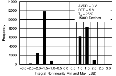
| INL | Integral linearity(5) | ADS8881C | –2 | ±1.2 | 2 | LSB(2) | ||
| ADS8881I | –3 | ±1.5 | 3 | |||||
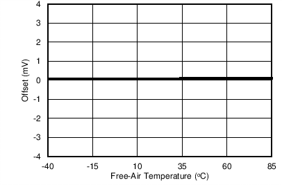
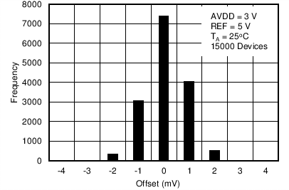
| EO | Offset error(3) | –4 | ±1 | 4 | mV | |||
| Offset error drift with temperature | ±1.5 | µV/°C | ||||||
| EG | Gain error | –0.01 | ±0.005 | 0.01 | %FSR | |||
| Gain error drift with temperature | ±0.15 | ppm/°C | ||||||
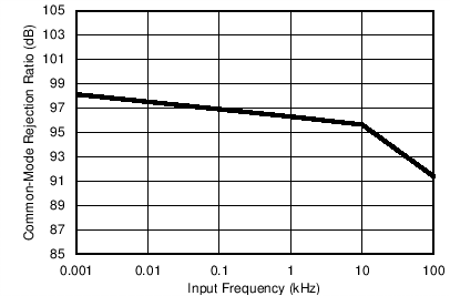
| CMRR | Common-mode rejection ratio | 90 | 100 | dB | ||||
| PSRR | Power-supply rejection ratio | At mid-code | 80 | dB | ||||
| Transition noise | 0.7 | LSB | ||||||
| SAMPLING DYNAMICS | ||||||||
| tconv | Conversion time | 500 | 710 | ns | ||||
| tACQ | Acquisition time | 290 | ns | |||||
| Maximum throughput rate with or without latency |
1000 | kHz | ||||||
| Aperture delay | 4 | ns | ||||||
| Aperture jitter, RMS | 5 | ps | ||||||
| Step response | Settling to 18-bit accuracy | 290 | ns | |||||
| Overvoltage recovery | Settling to 18-bit accuracy | 290 | ns | |||||
| DYNAMIC CHARACTERISTICS | ||||||||
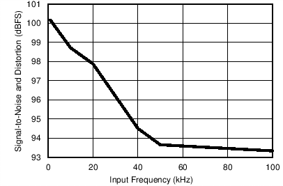
| SINAD | Signal-to-noise + distortion(7) | At 1 kHz, VREF = 5 V | 98 | 99.9 | dB | |||
| At 10 kHz, VREF = 5 V | 98.7 | |||||||
| At 100 kHz, VREF = 5 V | 93.3 | |||||||
| SNR | Signal-to-noise ratio(7) | At 1 kHz, VREF = 5 V | 98.5 | 100 | dB | |||
| At 10 kHz, VREF = 5 V | 99.5 | |||||||
| At 100 kHz, VREF = 5 V | 93.5 | |||||||
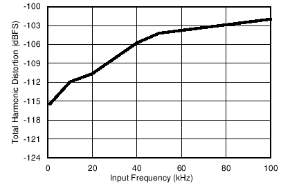
| THD | Total harmonic distortion(7)(4) | At 1 kHz, VREF = 5 V | –115 | dB | ||||
| At 10 kHz, VREF = 5 V | –112 | |||||||
| At 100 kHz, VREF = 5 V | –102 | |||||||
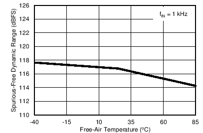
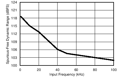
| SFDR | Spurious-free dynamic range(7) | At 1 kHz, VREF = 5 V | 115 | dB | ||||
| At 10 kHz, VREF = 5 V | 112 | |||||||
| At 100 kHz, VREF = 5 V | 102 | |||||||
| BW–3dB | –3-dB small-signal bandwidth | 30 | MHz | |||||
| POWER-SUPPLY REQUIREMENTS | ||||||||
| Power-supply voltage | AVDD | Analog supply | 2.7 | 3 | 3.6 | V | ||
| DVDD | Digital supply range for SCLK > 40 MHz | 2.7 | 3 | 3.6 | ||||
| Digital supply range for SCLK < 40 MHz | 1.65 | 1.8 | 3.6 | |||||
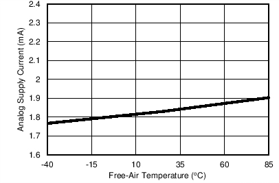
| Supply current | AVDD | 1-MHz sample rate, AVDD = 3 V | 1.8 | 2.4 | mA | |||
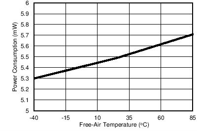
| PVA | Power dissipation | 1-MHz sample rate, AVDD = 3 V | 5.5 | 7.2 | mW | |||
| 100-kHz sample rate, AVDD = 3 V | 0.55 | |||||||
| 10-kHz sample rate, AVDD = 3 V | 55 | μW | ||||||
| IAPD | Device power-down current(6) | 50 | nA | |||||
| DIGITAL INPUTS: LOGIC FAMILY (CMOS) | ||||||||
| VIH | High-level input voltage | 1.65 V < DVDD < 2.3 V | 0.8 × DVDD | DVDD + 0.3 | V | |||
| 2.3 V < DVDD < 3.6 V | 0.7 × DVDD | DVDD + 0.3 | ||||||
| VIL | Low-level input voltage | 1.65 V < DVDD < 2.3 V | –0.3 | 0.2 × DVDD | V | |||
| 2.3 V < DVDD < 3.6 V | –0.3 | 0.3 × DVDD | ||||||
| ILK | Digital input leakage current | ±10 | ±100 | nA | ||||
| DIGITAL OUTPUTS: LOGIC FAMILY (CMOS) | ||||||||
| VOH | High-level output voltage | IO = 500-μA source, CLOAD = 20 pF | 0.8 × DVDD | DVDD | V | |||
| VOL | Low-level output voltage | IO = 500-μA sink, CLOAD = 20 pF | 0 | 0.2 × DVDD | V | |||
| TEMPERATURE RANGE | ||||||||
| TA | Operating free-air temperature | ADS8881C | 0 | 70 | °C | |||
| ADS8881I | –40 | 85 | ||||||
8.6 Timing Requirements: 3-Wire Operation
All specifications are at AVDD = 3 V, DVDD = 3 V, and over the operating free-air temperature range, unless otherwise noted. Figure 1. 3-Wire Operation: CONVST Functions as Chip Select
NOTE: Figure 1 shows the timing diagram for the 3-Wire CS Mode Without a Busy Indicator interface option. However, the timing parameters specified in Timing Requirements: 3-Wire Operation are also applicable for the 3-Wire CS Mode With a Busy Indicator interface option, unless otherwise specified; see the Device Functional Modes section for specific details for each interface option.
8.7 Timing Requirements: 4-Wire Operation
All specifications are at AVDD = 3 V, DVDD = 3 V, and over the operating free-air temperature range, unless otherwise noted.| MIN | TYP | MAX | UNIT | |||
|---|---|---|---|---|---|---|
| tACQ | Acquisition time | 290 | ns | |||
| tconv | Conversion time | TA in the range –40°C to 85°C | 500 | 710 | ns | |
| TA in the range 0°C to 70°C | 500 | 700 | ||||
| tconv | Conversion time | 500 | ns | |||
| 1/fsample | Time between conversions | 1000 | ns | |||
| twh-DI | Pulse duration: DIN high | 10 | ns | |||
| twl-CNV | Pulse width: CONVST low | 20 | ns | |||
| td-DI-DO | Delay time: DIN low to MSB valid | 12.3 | ns | |||
| td-DI-DOhz | Delay time: DIN high or last SCLK falling edge to DOUT 3-state | 13.2 | ns | |||
| tsu-DI-CNV | Setup time: DIN high to CONVST rising edge | 7.5 | ns | |||
| th-DI-CNV | Hold time: DIN high from CONVST rising edge (see Figure 63) | 0 | ns | |||
 Figure 2. 4-Wire Operation: DIN Functions as Chip Select
NOTE: Figure 2 shows the timing diagram for the 4-Wire CS Mode Without a Busy Indicator interface option. However, the timing parameters specified in Timing Requirements: 4-Wire Operation are also applicable for the 4-Wire CS Mode With a Busy Indicator interface option, unless otherwise specified; see the Device Functional Modes section for specific details for each interface option.
8.8 Timing Requirements: Daisy-Chain
All specifications are at AVDD = 3 V, DVDD = 3 V, and over the operating free-air temperature range, unless otherwise noted.| MIN | TYP | MAX | UNIT | |||
|---|---|---|---|---|---|---|
| tACQ | Acquisition time | 290 | ns | |||
| tconv | Conversion time | TA in the range -40°C to 85°C | 500 | 710 | ns | |
| TA in the range 0°C to 70°C | 500 | 700 | ||||
| tconv | Conversion time | 500 | ns | |||
| 1/fsample | Time between conversions | 1000 | ns | |||
| tsu-CK-CNV | Setup time: SCLK valid to CONVST rising edge | 5 | ns | |||
| th-CK-CNV | Hold time: SCLK valid from CONVST rising edge | 5 | ns | |||
| tsu-DI-CNV | Setup time: DIN low to CONVST rising edge (see Figure 2) | 7.5 | ns | |||
| th-DI-CNV | Hold time: DIN low from CONVST rising edge (see Figure 63) | 0 | ns | |||
| tsu-DI-CK | Setup time: DIN valid to SCLK falling edge | 1.5 | ns | |||
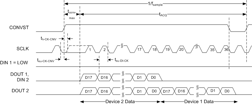 Figure 3. Daisy-Chain Operation: Two Devices
NOTE: Figure 3 shows the timing diagram for the Daisy-Chain Mode Without a Busy Indicator interface option. However, the timing parameters specified in Timing Requirements: Daisy-Chain are also applicable for the Daisy-Chain Mode With a Busy Indicator interface option, unless otherwise specified; see the Device Functional Modes section for specific details for each interface option.
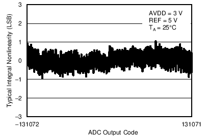
8.9 Typical Characteristics
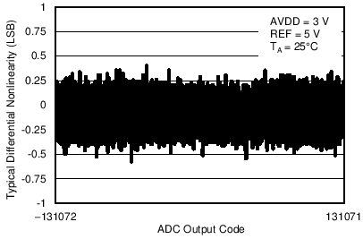
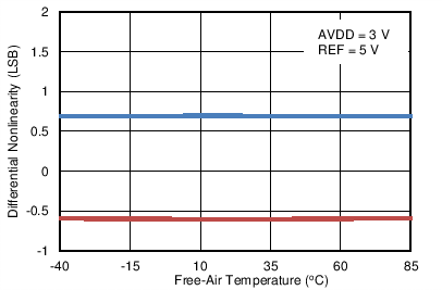
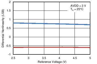
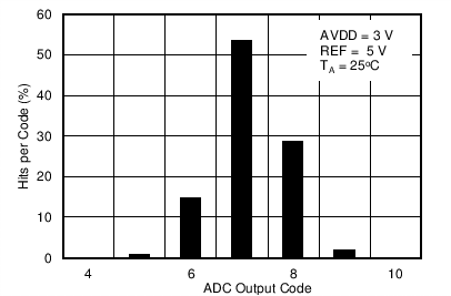
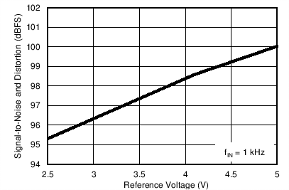
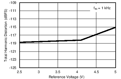
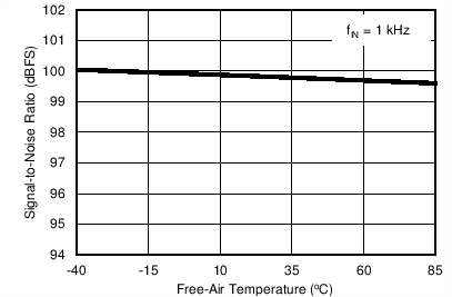
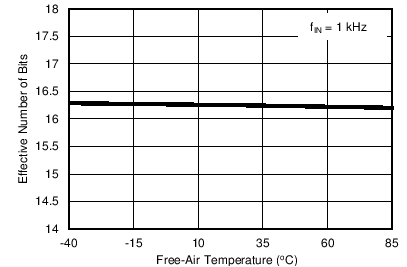
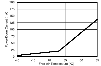
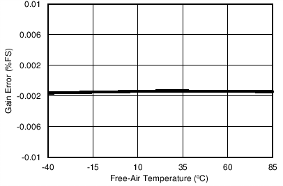
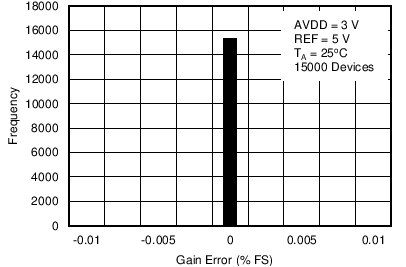
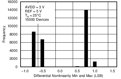
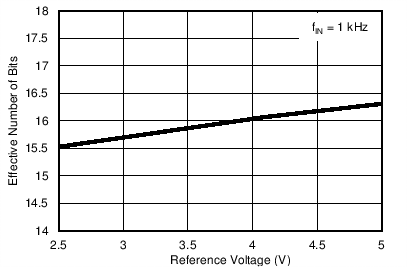
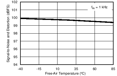
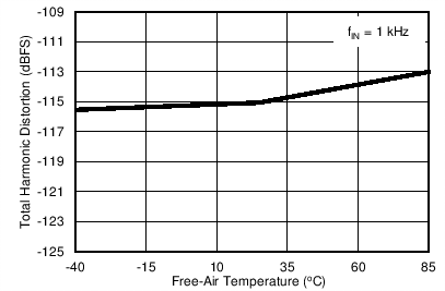
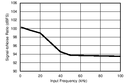
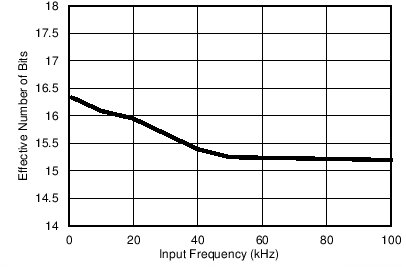
At TA = 25°C, AVDD = 3 V, DVDD = 3 V, VREF = 5 V, and fSAMPLE = 1 MSPS, unless otherwise noted.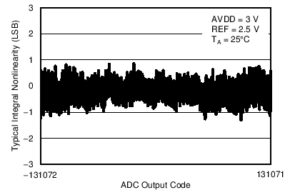
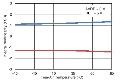
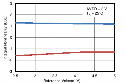
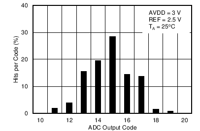
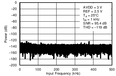
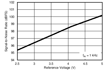


Nonlinearity (Minimum and Maximum)

