SBAS619A March 2014 – June 2017 AFE5401-Q1
PRODUCTION DATA.
- 1 Features
- 2 Applications
- 3 Description
- 4 Revision History
- 5 Pin Configuration and Functions
-
6 Specifications
- 6.1 Absolute Maximum Ratings
- 6.2 ESD Ratings
- 6.3 Recommended Operating Conditions
- 6.4 Thermal Information
- 6.5 Electrical Characteristics
- 6.6 Digital Characteristics
- 6.7 Timing Requirements: Output Interface
- 6.8 Timing Requirements: RESET
- 6.9 Timing Requirements: Serial Interface Operation
- 6.10 Typical Characteristics
- 7 Parameter Measurement Information
- 8 Timing Requirements: Across Output Serialization Modes
-
9 Detailed Description
- 9.1 Overview
- 9.2 Functional Block Diagram
- 9.3 Feature Description
- 9.4 Device Functional Modes
- 9.5 Programming
- 9.6 Register Maps
- 10Application and Implementation
- 11Power Supply Recommendations
- 12Layout
- 13Device and Documentation Support
- 14Mechanical, Packaging, and Orderable Information
Package Options
Mechanical Data (Package|Pins)
- RGC|64
Thermal pad, mechanical data (Package|Pins)
- RGC|64
Orderable Information
10 Application and Implementation
NOTE
Information in the following applications sections is not part of the TI component specification, and TI does not warrant its accuracy or completeness. TI’s customers are responsible for determining suitability of components for their purposes. Customers should validate and test their design implementation to confirm system functionality.
10.1 Application Information
The AFE5401-Q1 is a quad-channel, analog front-end (AFE), targeting applications where the level of integration is critical. Each channel comprises a complete base-band signal chain with:
- A low-noise amplifier (LNA),
- A programmable equalizer (EQ),
- A programmable gain amplifier (PGA), and
- An antialias filter (AAF)
- A high-speed, 12-bit, analog-to-digital converter (ADC) that samples at 25 MSPS per channel.
Having four integrated signal chain channels enables the device to be used in different end-use systems such as:
- Automotive radar (where a down-converted base-band signal from an RF front-end can be applied to the inputs of the AFE)
- Applications where up to 12-MHz voltage signal is available from a transducer
10.2 Typical Application
As Figure 122 illustrates, the device also consists of four auxiliary channels, where the analog signal chain (LNA, PGA) is bypassed and the analog inputs can be directly digitized. This configuration is very useful in the system to digitize monitoring signals (such as battery voltages and temperature sensor outputs).
As the Design Requirements section describes, the device can accept a variety of input clock signals (such as differential sine-wave, LVPECL, or LVDS). The can also functions seamlessly with a single-ended LVCMOS (1.8 V) clock input.
The device is designed to have a simple CMOS output data interface. Used with the TRIG and DSYNCx signals, the device can be interfaced to standard video ports of DSPs and other field-programmable gate array (FPGA) and micro-controller based receivers.
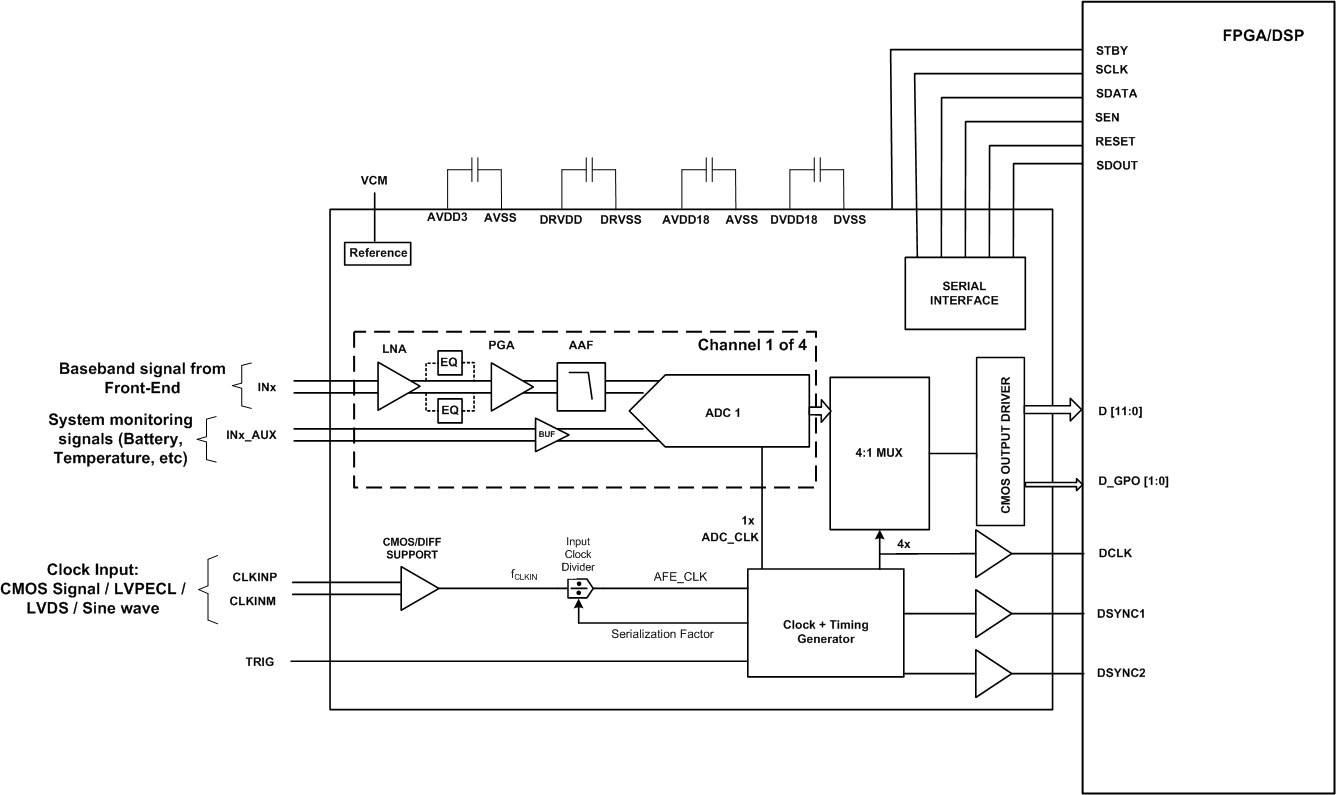 Figure 122. Typical Application Diagram
10.2.1 Design Requirements
The device can operate with either single-ended (CMOS) or differential input clocks (such as sine wave, LVPECL, and LVDS). Operating with a low-jitter differential clock is recommended for good SNR performance. In differential mode, the clock inputs are internally biased to the optimum common-mode voltage (approximately 0.95 V). While driving with an external LVPECL or LVDS driver, TI recommends ac-coupling the clock signals because the clock pins are internally biased to the common-mode voltage.
10.2.2 Detailed Design Procedure
For the LVDS input clock, RTERM = 100 Ω is recommended. For the LVPECL clock input, RTERM must be determined based on the LVPECL driver recommendations. To operate using a single-ended clock, connect a CMOS clock source to CLKINP and tie CLKINM to GND. The device automatically detects the presence of a single-ended clock without requiring any configuration and disables internal biasing. Typical clock termination schemes are illustrated in Figure 125, Figure 126, Figure 127, and Figure 128. Typical characteristic plots across input clock amplitude and duty cycle are shown in Application Curves.
Figure 123 and Figure 124 illustrate the equivalent circuits of the clock input pins for Differential and Single-Ended input clock respectively.
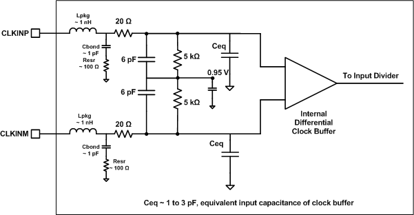 Figure 123. Clock Input Equivalent Circuit (Differential Mode)
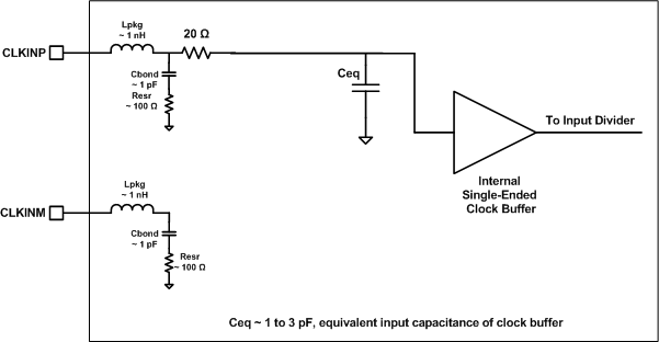 Figure 124. Clock Input Equivalent Circuit (Single-Ended Mode)
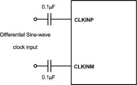 Figure 125. Differential Sine-Wave Clock
 Driving Circuit
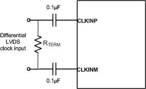 Figure 127. Differential LVDS Clock Driving Circuit
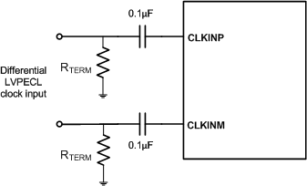 Figure 126. Differential LVPECL Clock
 Driving Circuit
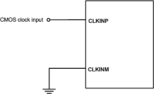 Figure 128. Single-Ended Clock Driving Circuit
10.2.3 Application Curves
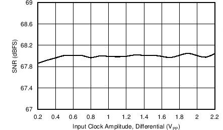 Figure 129. Signal-to-Noise Ratio vs Input Clock Amplitude (PGA Gain = 0 dB)
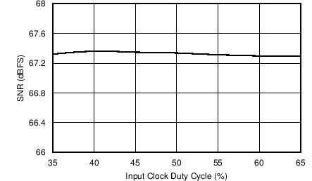 Figure 130. Signal-to-Noise Ratio vs Input Clock Duty Cycle (PGA Gain = 0 dB)