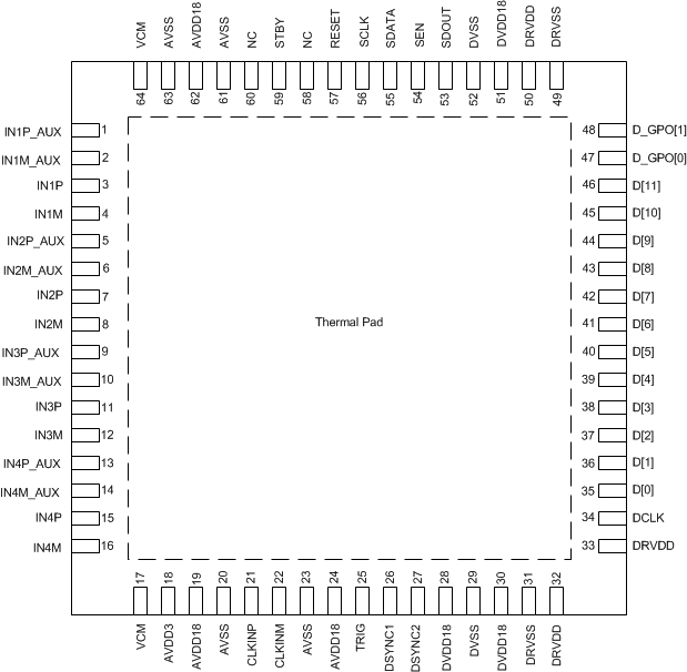
| D[11:0] |
35-46 |
CMOS outputs for channels 1 to 4 |
| D_GPO[1:0] |
47, 48 |
General-purpose CMOS output |
| AVDD3 |
18 |
3.3-V analog supply voltage |
| AVDD18 |
19, 24, 62 |
1.8-V analog supply voltage |
| AVSS |
20, 23, 61, 63 |
Analog ground |
| CLKINM |
22 |
Negative differential clock input pin. A single-ended clock is also supported. |
| CLKINP |
21 |
Positive differential clock input pin. A single-ended clock is also supported. |
| DCLK |
34 |
CMOS output clock |
| DRVDD |
32, 33, 50 |
CMOS output driver supply |
| DRVSS |
31, 49 |
CMOS output driver ground |
| DSYNC1 |
26 |
Data synchronization clock 1 |
| DSYNC2 |
27 |
Data synchronization clock 2 |
| DVDD18 |
28, 30, 51 |
1.8-V digital supply voltage |
| DVSS |
29, 52 |
Digital ground |
| IN1M |
4 |
Negative differential analog input pin for channel 1 |
| IN1P |
3 |
Positive differential analog input pin for channel 1 |
| IN1M_AUX |
2 |
Negative differential auxiliary analog input pin for channel 1 |
| IN1P_AUX |
1 |
Positive differential auxiliary analog input pin for channel 1 |
| IN2M |
8 |
Negative differential analog input pin for channel 2 |
| IN2P |
7 |
Positive differential analog input pin for channel 2 |
| IN2M_AUX |
6 |
Negative differential auxiliary analog input pin for channel 2 |
| IN2P_AUX |
5 |
Positive differential auxiliary analog input pin for channel 2 |
| IN3M |
12 |
Negative differential analog input pin for channel 3 |
| IN3P |
11 |
Positive differential analog input pin for channel 3 |
| IN3M_AUX |
10 |
Negative differential auxiliary analog input pin for channel 3 |
| IN3P_AUX |
9 |
Positive differential auxiliary analog input pin for channel 3 |
| IN4M |
16 |
Negative differential analog input pin for channel 4 |
| IN4P |
15 |
Positive differential analog input pin for channel 4 |
| IN4P_AUX |
13 |
Positive differential auxiliary analog input pin for channel 4 |
| IN4M_AUX |
14 |
Negative differential auxiliary analog input pin for channel 4 |
| NC |
58, 60 |
Do not connect |
| RESET |
57 |
Hardware reset pin (active high). This pin has an internal 150-kΩ pull-down resistor. |
| SCLK |
56 |
Serial interface clock input. This pin has an internal 150-kΩ pull-down resistor. |
| SDATA |
55 |
Serial interface data input. This pin has an internal 150-kΩ pull-down resistor. |
| SDOUT |
53 |
Serial interface data readout |
| SEN |
54 |
Serial interface enable. This pin has an internal 150-kΩ pull-up resistor. |
| STBY |
59 |
Standby control input. This pin has an internal 150-kΩ pull-down resistor. |
| TRIG |
25 |
Trigger for DSYNC1 and DSYNC2. This pin has an internal 150-kΩ pull-down resistor. |
| VCM |
17, 64 |
Output pins for common-mode bias voltage of the auxiliary input signals |
| Thermal pad |
Pad |
Located on bottom of package, internally connected to AVSS. Connect to ground plane on the board. |
