SBAS619A March 2014 – June 2017 AFE5401-Q1
PRODUCTION DATA.
- 1 Features
- 2 Applications
- 3 Description
- 4 Revision History
- 5 Pin Configuration and Functions
-
6 Specifications
- 6.1 Absolute Maximum Ratings
- 6.2 ESD Ratings
- 6.3 Recommended Operating Conditions
- 6.4 Thermal Information
- 6.5 Electrical Characteristics
- 6.6 Digital Characteristics
- 6.7 Timing Requirements: Output Interface
- 6.8 Timing Requirements: RESET
- 6.9 Timing Requirements: Serial Interface Operation
- 6.10 Typical Characteristics
- 7 Parameter Measurement Information
- 8 Timing Requirements: Across Output Serialization Modes
-
9 Detailed Description
- 9.1 Overview
- 9.2 Functional Block Diagram
- 9.3 Feature Description
- 9.4 Device Functional Modes
- 9.5 Programming
- 9.6 Register Maps
- 10Application and Implementation
- 11Power Supply Recommendations
- 12Layout
- 13Device and Documentation Support
- 14Mechanical, Packaging, and Orderable Information
Package Options
Mechanical Data (Package|Pins)
- RGC|64
Thermal pad, mechanical data (Package|Pins)
- RGC|64
Orderable Information
6 Specifications
6.1 Absolute Maximum Ratings
over operating free-air temperature range (unless otherwise noted)(1)| MIN | MAX | UNIT | ||
|---|---|---|---|---|
| Voltage range | DRVDD to DRVSS | –0.3 | +3.8 | V |
| AVDD3 to AVSS | –0.3 | +3.8 | ||
| AVDD18 to AVSS | –0.3 | +2.2 | ||
| DVDD18 to DVSS | –0.3 | +2.2 | ||
| Voltage between | AVSS and DVSS | –0.3 | +0.3 | V |
| AVSS and DRVSS | –0.3 | +0.3 | ||
| DVSS and DRVSS | –0.3 | +0.3 | ||
| Clock input pins (CLKINP and CLKINM) to AVSS | –0.3 | minimum (2.2, AVDD18 + 0.3) | V | |
| Analog input pins (INIP, INIM, INIP_AUX, and INIM_AUX) to AVSS | –0.3 | minimum (2.2, AVDD18 + 0.3) | V | |
| Digital control pins to DVSS | STBY, RESET, SCLK, SDATA, SEN, TRIG | –0.3 | +3.6 | V |
| Maximum operating junction temperature, TJ max | +125 | °C | ||
| Storage temperature, Tstg | –60 | +150 | °C | |
(1) Stresses beyond those listed under Absolute Maximum Ratings may cause permanent damage to the device. These are stress ratings only, and do not imply functional operation of the device at these or any other conditions beyond those indicated under Recommended Operating Conditions. Exposure to absolute-maximum-rated conditions for extended periods may affect device reliability.
6.2 ESD Ratings
| VALUE | UNIT | |||
|---|---|---|---|---|
| V(ESD) | Electrostatic discharge | Human-body model (HBM), per AEC Q100-002(1) | ±1000 | V |
| Charged-device model (CDM), per AEC Q100-011 | ±500 | |||
(1) AEC Q100-002 indicates that HBM stressing shall be in accordance with the ANSI/ESDA/JEDEC JS-001 specification.
6.3 Recommended Operating Conditions
| MIN | NOM | MAX | UNIT | |||
|---|---|---|---|---|---|---|
| TEMPERATURE | ||||||
| TA | Ambient temperature range | –40 | +105 | °C | ||
| SUPPLIES | ||||||
| DRVDD | Output driver supply | 1.7 | 3.6 | V | ||
| AVDD3 | 3-V analog supply voltage | 3 | 3.3 | 3.6 | V | |
| AVDD18 | 1.8-V analog supply voltage | 1.7 | 1.8 | 1.9 | V | |
| DVDD18 | 1.8-V digital supply voltage | 1.7 | 1.8 | 1.9 | V | |
| CLOCK INPUT | ||||||
| CLKIN | Input clock frequency | Default mode (DIV_EN disabled) | 12.5 | 25 | MHz | |
| With DIV_EN, DIV_FRC enabled and DIV_REG = 1 | 25 | 50 | ||||
| With DIV_EN, DIV_FRC enabled and DIV_REG = 2 | 37.5 | 75 | ||||
| With DIV_EN, DIV_FRC enabled and DIV_REG = 3 | 50 | 100 | ||||
| With decimate-by-2 or decimate-by-4 modes enabled (DIV_EN disabled)(1) | 12.5 | 50 | ||||
| VCLKINP – VCLKINM | Input clock amplitude differential | Sine wave, ac-coupled | 0.2 | 1.5 | VPP | |
| LVPECL, ac-coupled | 0.2 | 1.6 | ||||
| LVDS, ac-coupled | 0.2 | 0.7 | ||||
| Single-ended CMOS clock on CLKINP with CLKINM connected to AVSS | 1.8 | V | ||||
| Input clock duty cycle | 40% | 60% | ||||
| DIGITAL OUTPUT | ||||||
| CLOAD | Tolerable external load capacitance from each output pin to DRVSS | 5 | pF | |||
(1) In decimation mode, input clock frequency (CLKIN) can be scaled up to maximum of 200 MHz with the input divider.
6.4 Thermal Information
| THERMAL METRIC(1) | AFE5401-Q1 | UNIT | |
|---|---|---|---|
| RGC (VQFN) | |||
| 64 PINS | |||
| RθJA | Junction-to-ambient thermal resistance | 24.9 | °C/W |
| RθJC(top) | Junction-to-case (top) thermal resistance | 8.7 | °C/W |
| RθJB | Junction-to-board thermal resistance | 3.9 | °C/W |
| ψJT | Junction-to-top characterization parameter | 0.2 | °C/W |
| ψJB | Junction-to-board characterization parameter | 3.9 | °C/W |
| RθJC(bot) | Junction-to-case (bottom) thermal resistance | 0.5 | °C/W |
(1) For more information about traditional and new thermal metrics, see the Semiconductor and IC Package Thermal Metrics application report.
6.5 Electrical Characteristics
Minimum and maximum values are across the full temperature range of TMIN = –40°C to TMAX = +105°C, DRVDD = 3.3 V, AVDD3 = 3.3 V, AVDD18 = 1.8 V, DVDD18 = 1.8 V, –1-dBFS analog input ac-coupled with a 0.1-µF capacitor, AFE_CLK = 25 MHz, LNA gain = 15 dB, PGA gain = 0 dB, default mode, and differential input clock with 50% duty cycle, unless otherwise noted. Typical values are at TNOM = +25°C.| PARAMETER | TEST CONDITIONS | MIN | TYP | MAX | UNIT | |||
|---|---|---|---|---|---|---|---|---|
| FULL-CHANNEL CHARACTERISTICS | ||||||||
| Maximum differential input signal amplitude on INIP and INIM | LNA gain = 12 dB | 0.5 | VPP | |||||
| LNA gain = 15 dB (default) | 0.35 | |||||||
| LNA gain = 16.5 dB | 0.3 | |||||||
| LNA gain = 18 dB | 0.25 | |||||||
| Input resistance, from each input to internal dc bias level | Default | 1 ± 20% | kΩ | |||||
| TERM_INT_20K_LNA / TERM_INT_20K_AUX = 1 | 10 ± 20% | |||||||
| CI | Input capacitance | Differential input capacitance | 5.5 | pF | ||||
| VVCM | VCM output voltage | Voltage on VCM pins | 1.45 | V | ||||
| VCM output current capability | For 50-mV drop in VCM voltage | 3 | mA | |||||
| Gain matching | Across channels and devices | 0.15 | 1 | dB | ||||
| EG | Gain error | PGA gain = 30 dB | ± 0.6 | ± 1.4 | dB | |||
| EO | Offset error | PGA gain = 30 dB, 1 sigma value | ± 120 | LSB | ||||
| Input-referred noise voltage | fIN = 3 MHz, idle channel, PGA gain = 30 dB (default) | 2.9 | 3.8 | nV/√Hz | ||||
| fIN = 3 MHz, idle channel, PGA gain = 30 dB (HIGH_POW_LNA mode) |
2.5 | |||||||
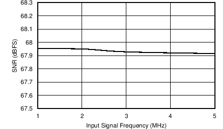
| SNR | Signal-to-noise ratio | fIN = 3 MHz, main channel | 65 | 67.7 | dBFS | |||
| fIN = 3 MHz, AUX channel | 69.2 | |||||||
| SFDR | Spurious-free dynamic range | fIN = 3 MHz, main channel (default) | 57 | 66 | dBc | |||
| fIN = 3 MHz, main channel (HPL_EN mode) | 74 | |||||||
| THD | Total harmonic distortion | fIN = 3 MHz, main channel | 56 | 65 | dBc | |||
| IMD | Intermodulation distortion | fIN1 = 1.5 MHz, fIN2 = 2 MHz, AIN1 and AIN2 = –7 dBFS | 83 | dBFS | ||||
| PSRR | Power-supply rejection ratio | For a 50-mVPP signal on AVDD18 up to 10 MHz, no input applied to analog inputs | > 50 | dB | ||||
| Number of bits in the ADC | 12 | Bits | ||||||
| Crosstalk, main channel to main channel | Aggressor channel: fIN = 2 MHz, 1 dB below ADC full-scale. Victim channel: fIN= 3 MHz, 1 dB below ADC full-scale. |
70 | dB | |||||
| Maximum channel gain | LNA gain = 18 dB, PGA gain = 30 dB | 48 | dB | |||||
| Minimum channel gain | LNA gain = 12 dB, PGA gain = 0 dB | 12 | dB | |||||
| PGA gain resolution | 3 | dB | ||||||
| PGA gain range | Maximum PGA gain – minimum PGA gain | 30 | dB | |||||
| Differential input voltage range for AUX channel | 2 | VPP | ||||||
| ANTIALIAS FILTER (Third-Order Elliptic) | ||||||||
| fC | 3-dB filter corner frequency | FILTER_BW = 0 (default) | 8 | MHz | ||||
| FILTER_BW = 1 | 7 | |||||||
| FILTER_BW = 2 | 10.5 | |||||||
| FILTER_BW = 3 | 12 | |||||||
| 3-dB filter corner frequency tolerance | For all FILTER_BW settings | ±5% | ||||||
| ATT2FC | Filter attenuation | At 2 × fC | 30 | dBc | ||||
| ATTSTPBND | Stop-band attenuation (fIN > 2.25 × fC) | 40 | ||||||
| RPPSBND | Ripple in pass band | 1.5 | dB | |||||
| POWER | ||||||||
| Total core power, per channel | Idle channel, excluding DRVDD power | 64 | mW | |||||
| IAVDD18 | AVDD18 current consumption | Default mode | 131 | 145 | mA | |||
| With HIGH_POW_LNA mode enabled | 153 | |||||||
| With HPL_EN mode enabled | 135 | |||||||
| IAVDD3 | AVDD3 current consumption | 1.5 | 3.5 | mA | ||||
| IDVDD18 | DVDD18 current consumption | 8 | 12 | mA | ||||
| IDRVDD | DRVDD current consumption | 5-pF load, toggle data test pattern mode | DRVDD = 3.3 V | 14 | mA | |||
| DRVDD = 1.8 V | 8.5 | |||||||
| 15-pF load, toggle data test pattern mode | DRVDD = 3.3 V | 36 | ||||||
| DRVDD = 1.8 V | 20 | |||||||
| Power-down | 5 | mW | ||||||
| STBY power | 15 | mW | ||||||
6.6 Digital Characteristics
The dc specifications refer to the condition where the digital outputs are not switching, but are permanently at a valid logic level 0 or 1. Minimum and maximum values are across the full temperature range of TMIN = –40°C to TMAX = +105°C, DRVDD = 3.3 V, AVDD3 = 3.3 V, AVDD18 = 1.8 V, and DVDD18 = 1.8 V, unless otherwise noted. Typical values are at TNOM = +25°C.| PARAMETER | MIN | TYP | MAX | UNIT | ||
|---|---|---|---|---|---|---|
| DIGITAL INPUTS (STBY, RESET, SCLK, CLKIN, SDATA, SEN, TRIG)(1) | ||||||
| VIH | High-level input voltage | 1.4 | V | |||
| VIL | Low-level input voltage | 0.4 | V | |||
| IIH | High-level input current | 10 | µA | |||
| IIL | Low-level input current | 10 | µA | |||
| CI | Input capacitance | 4 | pF | |||
| VIL_CLKINP | Input clock CMOS single-ended (VCLKINP), VCLKINM connected to AVSS | 0.25 × AVDD18 | V | |||
| VIH_CLKINP | 0.75 × AVDD18 | V | ||||
| DIGITAL OUTPUTS | ||||||
| VOH | High-level output voltage | DRVDD – 0.2 | DRVDD | V | ||
| VOL | Low-level output voltage | 0 | 0.2 | V | ||
(1) The SEN pin has an internal 150-kΩ pull-up resistor. The STBY, RESET, SCLK, SDATA, and TRIG pins have an internal 150-kΩ pull-down resistor.
6.7 Timing Requirements: Output Interface
Minimum and maximum values are across the full temperature range of TMIN = –40°C to TMAX = +105°C, DRVDD = 3.3 V, AVDD3 = 3.3 V, AVDD18 = 1.8 V, DVDD18 = 1.8 V, –1-dBFS analog input ac-coupled with 0.1 µF, AFE_CLK = 25 MHz, LNA gain = 15 dB, PGA gain = 0 dB, default mode, and differential input clock with 50% duty cycle, unless otherwise noted. Typical values are at TNOM = +25°C.| MIN | NOM | MAX | UNIT | |||
|---|---|---|---|---|---|---|
| tADLY | Aperture delay between the rising edge of the input sampling clock and the actual time at which the sampling occurs | 3 | ns | |||
| Wake-up time | Time to valid data after coming out of STANDBY mode | 500 | µs | |||
| Time to valid data after coming out of GLOBAL_PDN mode | 2 | ms | ||||
| Time to valid data after stopping and restarting the input clock | 500 | µs | ||||
| tLAT | ADC latency (default, after reset) | 10.5 | tAFE_CLK cycles | |||
| tSU | Data setup time | Data valid(1) to 50% of DCLK rising edge, DRVDD = 3.3 V, load = 5 pF, 4x serialization, STR_CTRL_CLK and STR_CTRL_CLK_DATA = 0 | 4.1 | ns | ||
| Data valid(1) to 50% of DCLK rising edge, DRVDD =1.8 V, load = 5 pF, 4x serialization, STR_CTRL_CLK and STR_CTRL_CLK_DATA = 5 | 3.7 | ns | ||||
| tHO | Data hold time | 50% of DCLK rising edge to data becoming invalid(1), DRVDD = 3.3 V, load = 5 pF, 4x serialization, STR_CTRL_CLK and STR_CTRL_CLK_DATA = 0 | 2.8 | ns | ||
| 50% of DCLK rising edge to data becoming invalid(1), DRVDD = 1.8 V, load = 5 pF, 4x serialization, STR_CTRL_CLK and STR_CTRL_CLK_DATA = 5 | 2.7 | ns | ||||
| tR, tF | CMOS output data and clock rise and fall time | DRVDD = 3.3 V, load = 5 pF, 10% to 90%, STR_CTRL_CLK and STR_CTRL_CLK_DATA = 0 | 1.2 | ns | ||
| DRVDD = 1.8 V, load = 5 pF, 10% to 90%, STR_CTRL_CLK and STR_CTRL_CLK_DATA = 5 | 1.1 | ns | ||||
| tOUT | Delay from CLKIN rising edge to DCLK rising edge, zero-crossing of input clock to 50% of DCLK rising edge, DRVDD = 3.3 V, load = 5 pF, 4x serialization, STR_CTRL_CLK and STR_CTRL_CLK_DATA = 0 | 6.7 | 9.5 | ns | ||
| tS_TRIG | TRIG setup time, TRIG pulse duration ≥ tAFE_CLK | 4 | ns | |||
| tH_TRIG | TRIG hold time, TRIG pulse duration ≥ tAFE_CLK | 3 | ns | |||
(1) Data valid refers to a logic high of 0.7 × DRVDD and a logic low of 0.3 × DRVDD.
6.8 Timing Requirements: RESET
Typical values are at TA = +25°C. Minimum and maximum specifications are across the full temperature range of TMIN = –40°C to TMAX = +105°C, DRVDD = 3.3 V, AVDD3 = 3.3 V, AVDD18 = 1.8 V, and DVDD18 = 1.8 V, unless otherwise noted.| PARAMETER | TEST CONDITIONS | MIN | TYP | MAX | UNIT | |
|---|---|---|---|---|---|---|
| t1 | Power-on to reset delay | Delay from power-up of AVDD18 and DVDD18 to RESET pulse active | 1 | ms | ||
| t2 | Reset pulse duration | Pulse duration of active RESET signal | 40 | ns | ||
| t3 | Register write delay | Delay from RESET disable to SEN active | 100 | ns | ||
6.9 Timing Requirements: Serial Interface Operation
Minimum specifications are across the full temperature range of TMIN = –40°C to TMAX = +105°C, DRVDD = 3.3 V, AVDD3 = 3.3 V, AVDD18 = 1.8 V, and DVDD18 = 1.8 V, CLOAD on SDOUT = 5 pF, unless otherwise noted.| PARAMETER | MIN | TYP | MAX | UNIT | |
|---|---|---|---|---|---|
| t1 | SCLK period | 50 | ns | ||
| t2 | SCLK high time | 20 | ns | ||
| t3 | SCLK low time | 20 | ns | ||
| t4 | Data setup time | 5 | ns | ||
| t5 | Data hold time | 5 | ns | ||
| t6 | SEN falling to SCLK rising | 8 | ns | ||
| t7 | Time between last SCLK rising edge to SEN rising edge | 8 | ns | ||
| t8 | Delay from SCLK falling edge to SDOUT valid | 7 | 11 | 15 | ns |

1.
Figure 1. Output Interface Timing Diagram
NOINDENT:
tCLK = 1 / fCLKINA high pulse on the RESET pin is required for register initialization through the reset pin. Figure 2 shows the timing requirement for reset after power-up.
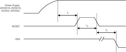 Figure 2. Reset Timing
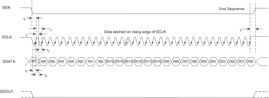 Figure 3. Serial Interface Register Write Timing Diagram
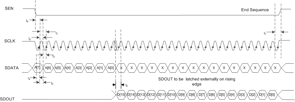 Figure 4. Serial Interface Register Readout Timing Diagram
6.10 Typical Characteristics
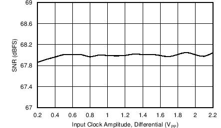
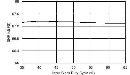
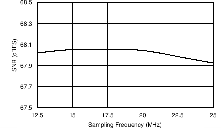
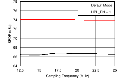
Typical values are at TA = +25°C, AVDD18 = DVDD18 = 1.8 V, AVDD3 = DRVDD = 3.3 V, –1-dBFS analog input ac-coupled with a 0.1-μF capacitor, AFE_CLK = 25 MHz, LNA gain = 15 dB, PGA gain = 0 dB, default mode, antialiasing filter corner frequency = 8 MHz, and differential input sine wave clock with 50% duty cycle, unless otherwise noted.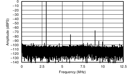
| SNR = 67.7 dBFS | SFDR = 65.7 dBc | THD = 65.2 dBc |
0-dB PGA Gain (Sample Rate = 25 MSPS)
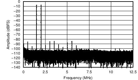
| fIN1 = 1.5 MHz | Each Tone at –7-dBFS Amplitude | |
| fIN2 = 2 MHz | Two-Tone IMD = –83 dBFS | |
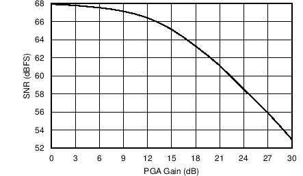
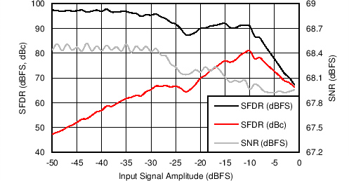
Spurious-Free Dynamic Range vs
Input Signal Amplitude (PGA Gain = 0 dB)
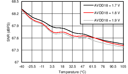
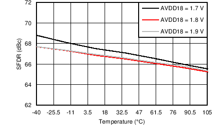

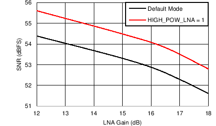
(PGA Gain = 30 dB)
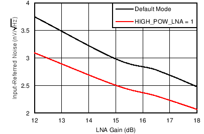
(PGA Gain = 30 dB)
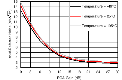
PGA Gain and Temperature
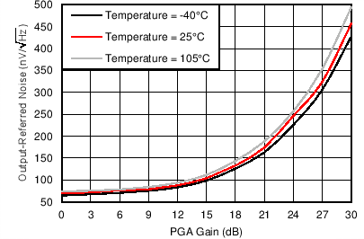
PGA Gain and Temperature
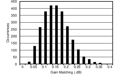
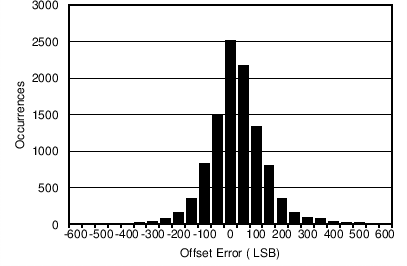
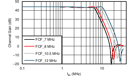
FILTER_BW Settings (PGA Gain = 30 dB)
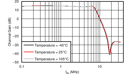
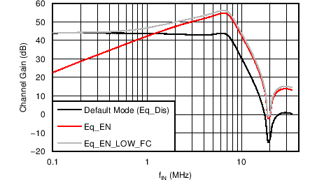
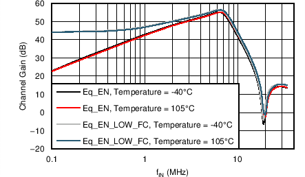
Equalizer Modes across Temperature (PGA Gain = 30 dB)
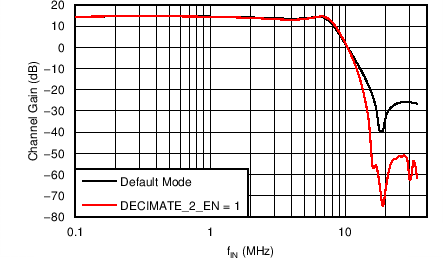
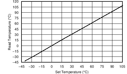
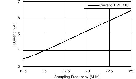
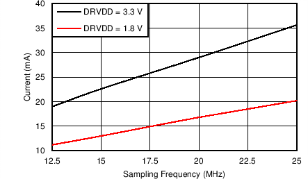
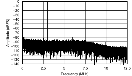
| SNR = 53.3 dBFS | SFDR = 63.7 dBc | THD = 63.6 dBc |
30-dB PGA Gain (Sample Rate = 25 MSPS)
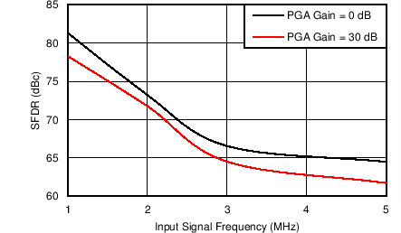
Input Signal Frequency
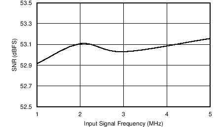
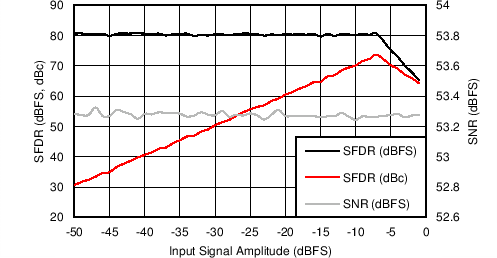
Spurious-Free Dynamic Range vs
Input Signal Amplitude (PGA Gain = 30 dB)
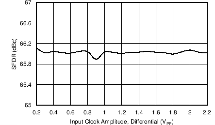
Input Clock Amplitude (PGA Gain = 0 dB)
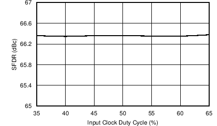
Input Clock Amplitude (PGA Gain = 0 dB)
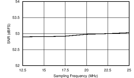
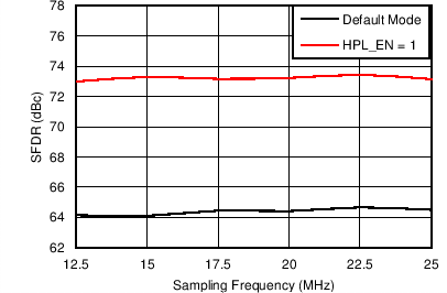
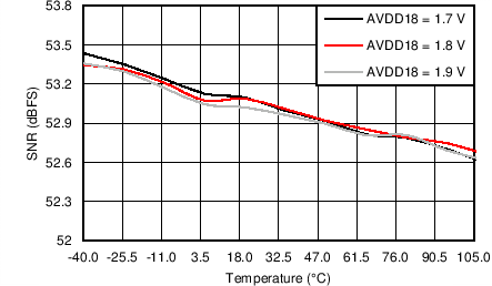
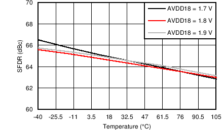
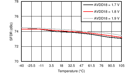
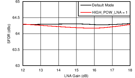
(PGA Gain = 30 dB)
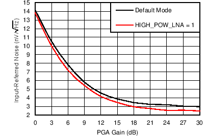
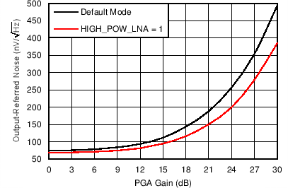
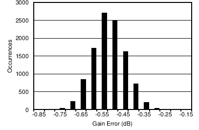
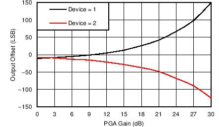
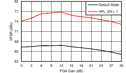
PGA Gain for Two Typical Devices
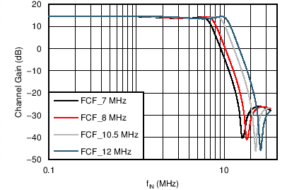
FILTER_BW Settings (PGA Gain = 0 dB)
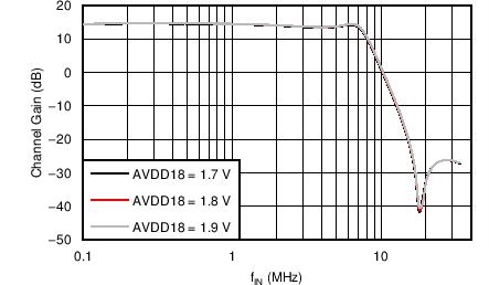
(PGA Gain = 0 dB, FILTER_BW = 8 MHz)
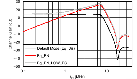
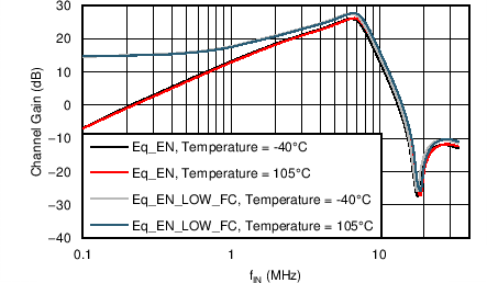
Equalizer Modes across Temperature (PGA Gain = 0 dB)
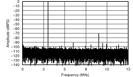
| SNR = 69.2 dBFS | SFDR = 69.8 dBc | THD = 69.7 dBc |
(3-MHz, –1-dBFS Input Signal, Sample Rate = 25 MSPS)
