Typical values at TA =
+25°C with nominal supplies. Default conditions: TX input data rate = 491.52MSPS,
fDAC = 11796.48MSPS (24x interpolation), interleave mode,
1st Nyquist zone output, PLL clock mode with fREF = 491.52
MHz, AOUT = –1 dBFS, DSA = 0 dB, Sin(x)/x enabled, DSA calibrated, TX
Clock Dither Enabled

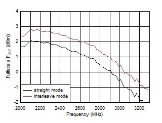
| Including PCB and cable losses, Aout =
-0.5dBFS, DSA = 0, 2.6 GHz matching |
|
Figure 6-78 TX
Full Scale vs RF Frequency at 11796.48MSPS
| fDAC=8847.36MSPS, straight mode,
matching at 2.6 GHz |
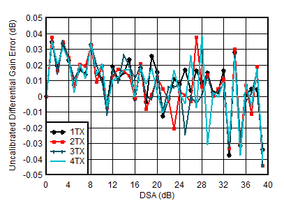
| Differential Gain Error = POUT(DSA Setting –
1) – POUT(DSA Setting) + 1 |
Figure 6-80 TX
Uncalibrated Differential Gain Error vs DSA Setting and Channel at 2.6
GHz
| fDAC=8847.36MSPS, straight mode,
matching at 2.6 GHz |
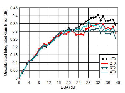
| Integrated Gain Error = POUT(DSA Setting) –
POUT(DSA Setting = 0) + (DSA
Setting) |
Figure 6-82 TX
Uncalibrated Integrated Gain Error vs DSA Setting and Channel at 2.6
GHz
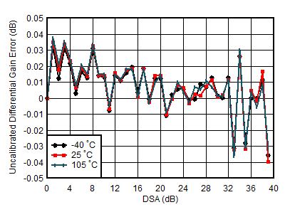
| fDAC = 8847.36MSPS, straight mode,
matching at 2.6 GHz, channel with the median variation
over DSA setting at 25°C |
| Differential Gain Error = POUT(DSA Setting –
1) – POUT(DSA Setting) + 1 |
Figure 6-84 TX
Uncalibrated Differential Gain Error vs DSA Setting and Temperature at 2.6
GHz
| fDAC = 8847.36MSPS, straight mode,
matching at 2.6 GHz, channel with the median variation
over DSA setting at 25°C |
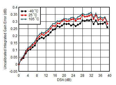
| Integrated Gain Error = POUT(DSA Setting) –
POUT(DSA Setting = 0) + (DSA
Setting) |
Figure 6-86 TX
Uncalibrated Integrated Gain Error vs DSA Setting and Temperature at 2.6
GHz
| fDAC = 8847.36MSPS, straight mode,
matching at 2.6 GHz |
| Differential Phase Error = PhaseOUT(DSA
Setting – 1) – PhaseOUT(DSA Setting) |
|
Figure 6-88 TX
Uncalibrated Differential Phase Error vs DSA Setting and Channel at 2.6
GHz
| fDAC = 8847.36MSPS, straight mode,
matching at 2.6 GHz |
| Integrated Phase Error = Phase(DSA Setting) – Phase(DSA
Setting = 0) |
Figure 6-90 TX
Uncalibrated Integrated Phase Error vs DSA Setting and Channel at 2.6
GHz
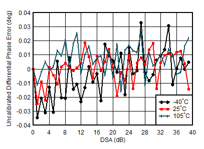
| fDAC = 8847.36MSPS, straight mode,
matching at 2.6 GHz, channel with the median variation
over DSA setting at 25°C |
| Differential Phase Error = PhaseOUT(DSA
Setting – 1) – PhaseOUT(DSA Setting) |
Figure 6-92 TX
Uncalibrated Differential Phase Error vs DSA Setting and Temperature at 2.6
GHz
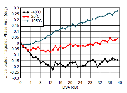
| fDAC = 8847.36MSPS, straight mode,
matching at 2.6 GHz, channel with the medium variation
over DSA setting at 25°C |
| Integrated Phase Error = Phase(DSA Setting) – Phase(DSA
Setting = 0) |
Figure 6-94 TX
Uncalibrated Integrated Phase Error vs DSA Setting and Temperature at 2.6
GHz
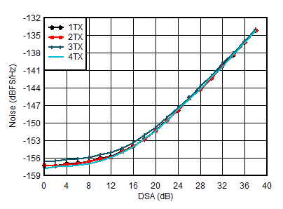
| fDAC = 8847.36MSPS, straight mode,
matching at 2.6 GHz, POUT = –13 dBFS |
Figure 6-96 TX
Output Noise vs Channel and Attenuation at 2.6 GHz
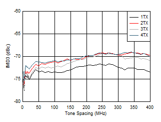
| fDAC = 8847.36MSPS, straight mode,
fCENTER = 2.6 GHz, matching at 2.6 GHz,
–13 dBFS each tone |
Figure 6-98 TX
IMD3 vs Tone Spacing and Channel at 2.6 GHz
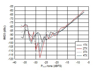
| fDAC = 8847.36MSPS, straight mode,
fCENTER = 2.6 GHz, fSPACING =
20 MHz, matching at 2.6 GHz |
Figure 6-100 TX
IMD3 vs Digital Level at 2.6 GHz
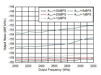
| Matching at 2.6 GHz, Single tone, fDAC =
11.79648GSPS, interleave mode, 40-MHz offset |
Figure 6-102 TX
Single Tone Output Noise vs Frequency and Amplitude at 2.6 GHz
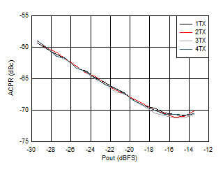
| Matching at 2.6 GHz, single carrier 20-MHz BW TM1.1
LTE |
Figure 6-104 TX
20-MHz LTE ACPR vs Digital Level at 2.6 GHz
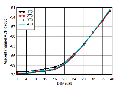
| Matching at 2.6 GHz, single carrier 20-MHz BW TM1.1
LTE |
Figure 6-106 TX
20-MHz LTE ACPR vs DSA at 2.6 GHz
| Matching at 2.6 GHz, single carrier 20-MHz BW TM1.1
LTE |
Figure 6-108 TX
20-MHz LTE ACPR vs DSA at 2.6 GHz
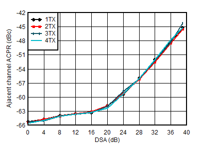
| Matching at 2.6 GHz, single carrier 100-MHz BW TM1.1
NR |
Figure 6-110 TX
100-MHz NR ACPR vs DSA at 2.6 GHz
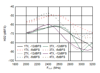
| Matching at 2.6 GHz, fDAC = 11.79648GSPS,
interleave mode, normalized to output power at harmonic
frequency |
Figure 6-112 TX
HD2 vs Digital Amplitude and Output Frequency at 2.6 GHz
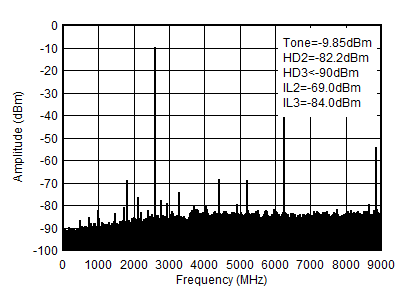
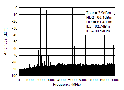
| fDAC = 8847.36MSPS, straight mode, 2.6
GHz matching, includes PCB and cable losses. ILn =
fS/n ± fOUT and is due to
mixing with digital clocks. |
Figure 6-114 TX
Single Tone (–12 dBFS) Output Spectrum at 2.6 GHz
(0-fDAC)
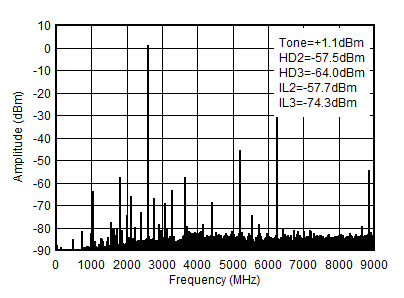
| fDAC = 8847.36MSPS, straight mode, 2.6
GHz matching, includes PCB and cable losses. ILn =
fS/n ± fOUT and is due to
mixing with digital clocks. |
Figure 6-116 TX
Single Tone (–1 dBFS) Output Spectrum at 2.6 GHz (0-fDAC)
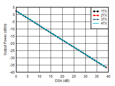
| fDAC = 8847.36 MSPS, Aout =
-0.5dBFS, matching 2.6 GHz |
|
|
Figure 6-79 TX
Output Power vs DSA Setting and Channel at 2.6 GHz
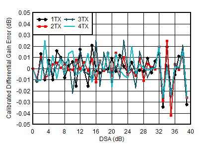
| fDAC=8847.36MSPS, straight mode,
matching at 2.6 GHz |
| Differential Gain Error = POUT(DSA Setting –
1) – POUT(DSA Setting) + 1 |
Figure 6-81 TX
Calibrated Differential Gain Error vs DSA Setting and Channel at 2.6
GHz
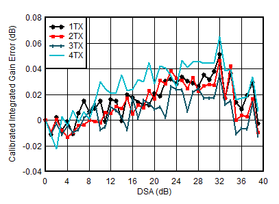
| fDAC = 8847.36MSPS, straight mode,
matching at 2.6 GHz |
| Integrated Gain Error = POUT(DSA Setting) –
POUT(DSA Setting = 0) + (DSA
Setting) |
|
Figure 6-83 TX
Calibrated Integrated Gain Error vs DSA Setting and Channel at 2.6
GHz
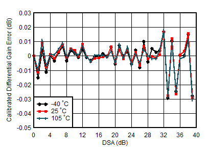
| fDAC = 8847.36MSPS, straight mode,
matching at 2.6 GHz, channel with the median variation
over DSA setting at 25°C |
| Differential Gain Error = POUT(DSA Setting –
1) – POUT(DSA Setting) + 1 |
Figure 6-85 TX
Calibrated Differential Gain Error vs DSA Setting and Temperature at 2.6
GHz
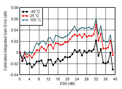
| fDAC = 8847.36MSPS, straight mode,
matching at 2.6 GHz, channel with the median variation
over DSA setting at 25°C |
| Integrated Gain Error = POUT(DSA Setting) –
POUT(DSA Setting = 0) + (DSA
Setting) |
Figure 6-87 TX
Calibrated Integrated Gain Error vs DSA Setting and Temperature at 2.6
GHz
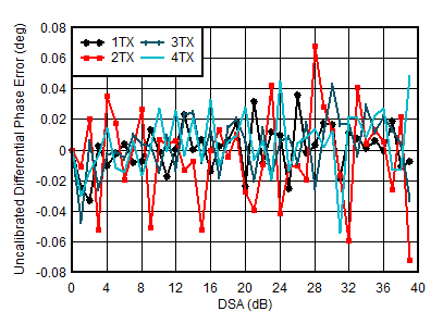
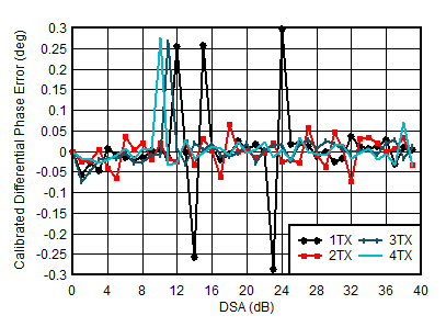
| fDAC = 8847.36MSPS, straight mode,
matching at 2.6 GHz |
| Differential Phase Error = PhaseOUT(DSA
Setting – 1) – PhaseOUT(DSA Setting) |
| Phase
DNL spike may occur at any DSA setting. |
Figure 6-89 TX
Calibrated Differential Phase Error vs DSA Setting and Channel at 2.6
GHz
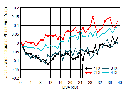
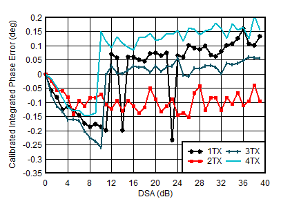
| fDAC = 8847.36MSPS, straight mode,
matching at 2.6 GHz |
| Integrated Phase Error = Phase(DSA Setting) – Phase(DSA
Setting = 0) |
|
Figure 6-91 TX
Calibrated Integrated Phase Error vs DSA Setting and Channel at 2.6
GHz
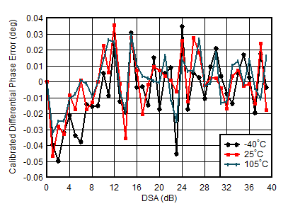
| fDAC = 8847.36MSPS, straight mode,
matching at 2.6 GHz, channel with the median variation
over DSA setting at 25°C |
| Differential Phase Error = PhaseOUT(DSA
Setting – 1) – PhaseOUT(DSA Setting) |
Figure 6-93 TX
Calibrated Differential Phase Error vs DSA Setting and Temperature at 2.6
GHz
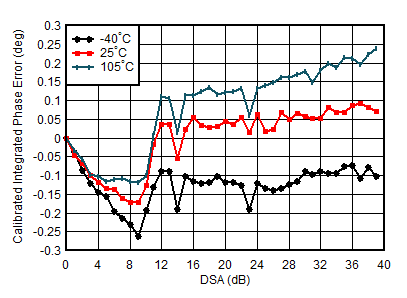
| fDAC = 8847.36MSPS, straight mode,
matching at 2.6 GHz, channel with the median variation
over DSA setting at 25°C |
| Integrated Phase Error = Phase(DSA Setting) – Phase(DSA
Setting = 0) |
Figure 6-95 TX
Calibrated Integrated Phase Error vs DSA Setting and Temperature at 2.6
GHz
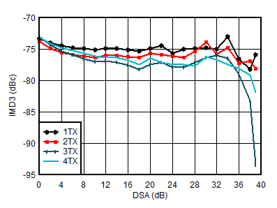
| fDAC = 8847.36MSPS, straight mode,
fCENTER = 2.6 GHz, matching at 2.6 GHz,
–13 dBFS each tone |
Figure 6-97 TX
IMD3 vs DSA Setting at 2.6 GHz
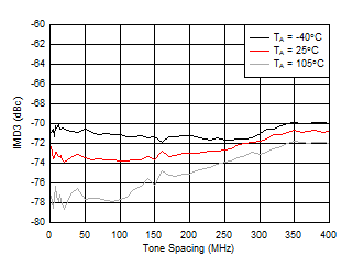
| fDAC = 8847.36MSPS, straight mode,
fCENTER = 2.6 GHz, matching at 2.6 GHz,
–13 dBFS each tone, worst channel. |
Figure 6-99 TX
IMD3 vs Tone Spacing and Temperature at 2.6 GHz
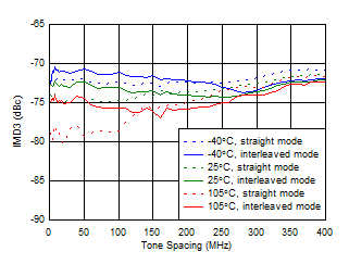
| fDAC = 8847.36MSPS, straight mode,
fCENTER = 2.6 GHz, matching at 2.6 GHz,
–13 dBFS each tone |
Figure 6-101 TX
IMD3 vs Tone Spacing and Temperature
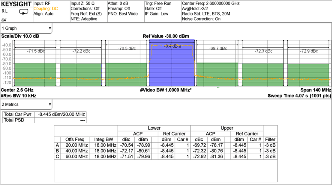
| TM1.1,
POUT_RMS = –13 dBFS |
|
|
|
Figure 6-103 TX
20-MHz LTE Output Spectrum at 2.6 GHz (Band 41)
| Matching at 2.6 GHz, single carrier 20-MHz BW TM1.1
LTE |
Figure 6-105 TX
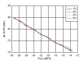
20-MHz LTE alt-ACPR vs Digital Level at 2.6 GHz
| Matching at 2.6 GHz, single carrier 20-MHz BW TM1.1
LTE |
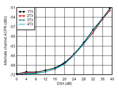
Figure 6-107 TX
20-MHz LTE alt-ACPR vs DSA at 2.6 GHz
| Matching at 2.6 GHz, single carrier 20-MHz BW TM1.1
LTE |
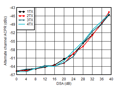
Figure 6-109 TX
20-MHz LTE alt-ACPR vs DSA at 2.6 GHz
| Matching at 2.6 GHz, single carrier 100-MHz BW TM1.1
NR |
|
Figure 6-111 TX
100-MHz NR alt-ACPR vs DSA at 2.6 GHz
| Matching at 2.6 GHz, fDAC = 11.79648GSPS,
interleave mode, normalized to output power at harmonic
frequency |
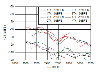
Figure 6-113 TX
HD3 vs Digital Amplitude and Output Frequency at 2.6 GHz
| fDAC = 8847.36MSPS, straight mode, 2.6
GHz matching, includes PCB and cable losses. ILn =
fS/n ± fOUT and is due to
mixing with digital clocks. |
Figure 6-115 TX
Single Tone (–6 dBFS) Output Spectrum at 2.6 GHz (0-fDAC)
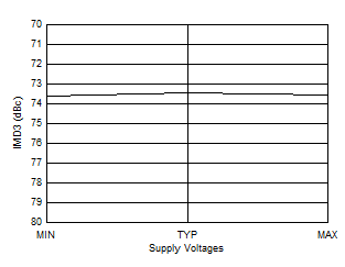
| fDAC = 11796.48MSPS, interleave mode,
2.6 GHz matching. 40-MHz offset from tone. Output Power
= –13 dBFS. All supplies simultaneously at MIN, TYP, or
MAX voltages. |
|
|
Figure 6-117 TX
IMD3 vs Supply Voltage at 2.6 GHz
