SBASA41D february 2021 – june 2023 AFE7950
PRODUCTION DATA
- 1
- 1Features
- 2Applications
- 3Description
- 4Description (continued)
- 5Revision History
-
6Specifications
- 6.1 Absolute Maximum Ratings
- 6.2 ESD Ratings
- 6.3 Recommended Operating Conditions
- 6.4 Thermal Information
- 6.5 Transmitter Electrical Characteristics
- 6.6 RF ADC Electrical Characteristics
- 6.7 PLL/VCO/Clock Electrical Characteristics
- 6.8 Digital Electrical Characteristics
- 6.9 Power Supply Electrical Characteristics
- 6.10 Timing Requirements
- 6.11 Switching Characteristics
- 6.12
Typical Characteristics
- 6.12.1 TX Typical Characteristics 800 MHz
- 6.12.2 TX Typical Characteristics at 1.8 GHz
- 6.12.3 TX Typical Characteristics at 2.6 GHz
- 6.12.4 TX Typical Characteristics at 3.5 GHz
- 6.12.5 TX Typical Characteristics at 4.9 GHz
- 6.12.6 TX Typical Characteristics at 8.1 GHz
- 6.12.7 TX Typical Characteristics at 9.6 GHz
- 6.12.8 RX Typical Characteristics at 800 MHz
- 6.12.9 RX Typical Characteristics at 1.75 GHz – 1.9 GHz
- 6.12.10 RX Typical Characteristics at 2.6 GHz
- 6.12.11 RX Typical Characteristics at 3.5 GHz
- 6.12.12 RX Typical Characteristics at 4.9 GHz
- 6.12.13 RX Typical Characteristics at 8.1GHz
- 6.12.14 RX Typical Characteristics at 9.6 GHz
- 6.12.15 PLL and Clock Typical Characteristics
- 7Device and Documentation Support
- 8Mechanical, Packaging, and Orderable Information
Package Options
Mechanical Data (Package|Pins)
Thermal pad, mechanical data (Package|Pins)
Orderable Information
3 Description
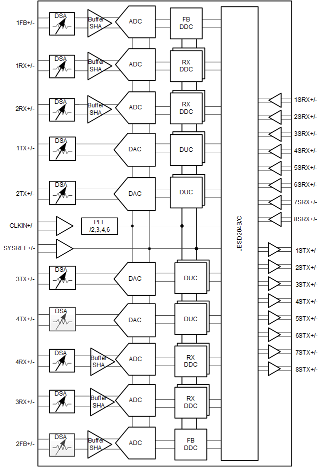
The AFE7950 is a high performance, wide bandwidth multi-channel transceiver, integrating four RF sampling transmitter chains, four RF sampling receiver chains and two RF sampling feedback chains (six RF sampling ADCs total). With operation up to 12 GHz, this device enables direct RF sampling in the L, S, C and X-band frequency ranges without the need for additional frequency conversions stages. This improvement in density and flexibility enables high-channel-count, multi-mission systems.
The TX signal paths support interpolation and digital up conversion options that deliver up to 1200 MHz of signal bandwidth for four TX or 2400 MHz for two TX. The output of the DUCs drives a 12-GSPS DAC (digital to analog converter) with a mixed mode output option to enhance 2nd Nyquist operation. The DAC output includes a variable gain amplifier (TX DSA) with 40-dB range and 1-dB analog and 0.125-dB digital steps.
 Functional Block Diagram