SBAS562B April 2012 – December 2019 AMC1100
PRODUCTION DATA.
- 1 Features
- 2 Applications
- 3 Description
- 4 Revision History
- 5 Pin Configuration and Functions
-
6 Specifications
- 6.1 Absolute Maximum Ratings
- 6.2 ESD Ratings
- 6.3 Recommended Operating Conditions
- 6.4 Thermal Information
- 6.5 Power Ratings
- 6.6 Insulation Specifications
- 6.7 Safety-Related Certifications
- 6.8 Safety Limiting Values
- 6.9 Electrical Characteristics
- 6.10 Insulation Characteristics Curves
- 6.11 Typical Characteristics
- 7 Detailed Description
- 8 Application and Implementation
- 9 Power Supply Recommendations
- 10Layout
- 11Device and Documentation Support
- 12Mechanical, Packaging, and Orderable Information
Package Options
Mechanical Data (Package|Pins)
Thermal pad, mechanical data (Package|Pins)
- DUB|8
Orderable Information
7.4 Device Functional Modes
The AMC1100 is powered on when the supplies are connected. The device is operated off a 5-V nominal supply on the high-side. The potential of the ground reference GND1 can be floating, which is usually the case in shunt-based current-measurement applications. TI recommends tying one side of the shunt to the GND1 pin of the AMC1100 to maintain the operating common-mode range requirements of the device.
The low-side of the AMC1100 can be powered from a supply source with a nominal voltage of 3.0 V, 3.3 V, or 5.0 V. When operated at 5 V, the common-mode voltage of the output stage is set to 2.55 V nominal; in both other cases, the common-mode voltage is automatically set to 1.29 V.
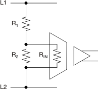
Although usually applied in shunt-based current-sensing circuits, the AMC1100 can also be used for isolated voltage measurement applications, as shown in a simplified way in Figure 34. In such applications, usually a resistor divider (R1 and R2 in Figure 34) is used to match the relatively small input voltage range of the AMC1100. R2 and the AMC1100 input resistance (RIN) also create a resistance divider that results in additional gain error. With the assumption that R1 and RIN have a considerably higher value than R2, the resulting total gain error can be estimated using Equation 1:

where
- GERR = device gain error.
 Figure 34. Voltage Measurement Application