SBAS562B April 2012 – December 2019 AMC1100
PRODUCTION DATA.
- 1 Features
- 2 Applications
- 3 Description
- 4 Revision History
- 5 Pin Configuration and Functions
-
6 Specifications
- 6.1 Absolute Maximum Ratings
- 6.2 ESD Ratings
- 6.3 Recommended Operating Conditions
- 6.4 Thermal Information
- 6.5 Power Ratings
- 6.6 Insulation Specifications
- 6.7 Safety-Related Certifications
- 6.8 Safety Limiting Values
- 6.9 Electrical Characteristics
- 6.10 Insulation Characteristics Curves
- 6.11 Typical Characteristics
- 7 Detailed Description
- 8 Application and Implementation
- 9 Power Supply Recommendations
- 10Layout
- 11Device and Documentation Support
- 12Mechanical, Packaging, and Orderable Information
Package Options
Mechanical Data (Package|Pins)
Thermal pad, mechanical data (Package|Pins)
- DUB|8
Orderable Information
9 Power Supply Recommendations
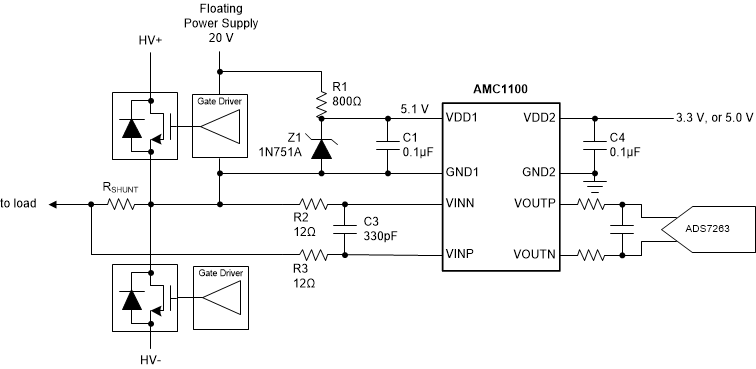
In a typical frequency inverter application, the high-side power supply for the AMC1100 (VDD1) is derived from the system supply, as shown in Figure 41. For lowest cost, a Zener diode can be used to limit the voltage to 5 V ± 10%. A 0.1-µF decoupling capacitor is recommended for filtering this power-supply path. Place this capacitor (C1) as close as possible to the VDD1 pin for best performance. If better filtering is required, an additional 1-µF to 10-µF capacitor can be used.
 Figure 41. Zener Diode Based High-Side Supply
 For higher power efficiency and better performance, a buck converter can be used; an example of such an approach is based on the LM5017. A reference design including performance test results and layout documentation can be downloaded at PMP9480, Isolated Bias Supplies + Isolated Amplifier Combo for Line Voltage or Current Measurement.