SBAS789B October 2017 – April 2020 AMC1106E05 , AMC1106M05
PRODUCTION DATA.
- 1 Features
- 2 Applications
- 3 Description
- 4 Revision History
- 5 Device Comparison Table
- 6 Pin Configuration and Functions
-
7 Specifications
- 7.1 Absolute Maximum Ratings
- 7.2 ESD Ratings
- 7.3 Recommended Operating Conditions
- 7.4 Thermal Information
- 7.5 Power Ratings
- 7.6 Insulation Specifications
- 7.7 Safety-Related Certifications
- 7.8 Safety Limiting Values
- 7.9 Electrical Characteristics: AMC1106x
- 7.10 Timing Requirements
- 7.11 Switching Characteristics
- 7.12 Insulation Characteristics Curves
- 7.13 Typical Characteristics
- 8 Detailed Description
- 9 Application and Implementation
- 10Power Supply Recommendations
- 11Layout
- 12Device and Documentation Support
- 13Mechanical, Packaging, and Orderable Information
Package Options
Mechanical Data (Package|Pins)
- DWV|8
Thermal pad, mechanical data (Package|Pins)
Orderable Information
8.3.1 Analog Input
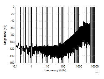
The AMC1106 incorporates front-end circuitry that contains a differential amplifier and sampling stage, followed by a ΔΣ modulator. The gain of the differential amplifier is set by internal precision resistors to a factor of 20 with a differential input resistance of 4.9 kΩ. For reduced offset and offset drift, the differential amplifier is chopper-stabilized with the switching frequency set at fCLKIN / 32. Figure 41 shows that the switching frequency generates a spur. The impact of this spur on the overall system-level performance depends on the digital filter settings.

| sinc3 filter, OSR = 2, fCLKIN = 20 MHz, fIN = 1 kHz |
There are two restrictions on the analog input signals (AINP and AINN). First, if the input voltage exceeds the range AGND – 6 V to AVDD + 0.5 V, the input current must be limited to 10 mA because the device input electrostatic discharge (ESD) diodes turn on. In addition, the linearity and noise performance of the device are ensured only when the differential analog input voltage remains within the specified linear full-scale range (FSR) and within the specified input common-mode voltage range (VCM).