SBAS512F April 2011 – February 2020 AMC1204
PRODUCTION DATA.
- 1 Features
- 2 Applications
- 3 Description
- 4 Revision History
- 5 Pin Configuration and Functions
-
6 Specifications
- 6.1 Absolute Maximum Ratings
- 6.2 ESD Ratings
- 6.3 Recommended Operating Conditions
- 6.4 Thermal Information
- 6.5 Power Ratings
- 6.6 Insulation Specifications
- 6.7 Safety-Related Certifications
- 6.8 Safety Limiting Values
- 6.9 Electrical Characteristics
- 6.10 Timing Requirements
- 6.11 Insulation Characteristics Curves
- 6.12 Typical Characteristics
- 7 Detailed Description
- 8 Application and Implementation
- 9 Power Supply Recommendations
- 10Layout
- 11Device and Documentation Support
- 12Mechanical, Packaging, and Orderable Information
Package Options
Mechanical Data (Package|Pins)
Thermal pad, mechanical data (Package|Pins)
- DW|16
Orderable Information
7.3.1 Analog Input
The differential analog input of the AMC1204 and AMC1204B is implemented with a switched-capacitor circuit.
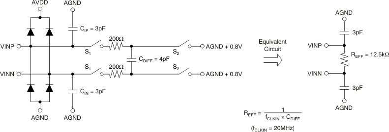
The AMC1204 and AMC1204B measure the differential input signal VIN = (VINP – VINN) against the internal reference of 2.5 V using internal capacitors that are continuously charged and discharged. Figure 44 shows the simplified schematic of the AMC1204 and AMC1204B input circuitry; the right side of Figure 44 illustrates the input circuitry with the capacitors and switches replaced by an equivalent circuit.
In Figure 44, the S1 switches close during the input sampling phase. With the S1 switches closed, CDIFF charges to the voltage difference across VINP and VINN. For the discharge phase, both S1 switches open first and then both S2 switches close. CDIFF discharges approximately to AGND + 0.8 V during this phase. This two-phase sample/discharge cycle repeats with a period of tCLKIN = 1/fCLKIN. fCLKIN is the operating frequency of the modulator. The capacitors CIP and CIN are of parasitic nature and caused by bonding wires and the internal ESD protection structure.
 Figure 44. Equivalent Analog Input Circuit
 There are two restrictions on the analog input signals VINP and VINN. First, if the input voltage exceeds the range AGND – 0.5 V to AVDD + 0.3 V, the input current must be limited to 10 mA because the input protection diodes on the front end of the converter begin to turn on. In addition, the linearity and the noise performance of the device are ensured only when the differential analog input voltage remains within ±250 mV.