SBAS512F April 2011 – February 2020 AMC1204
PRODUCTION DATA.
- 1 Features
- 2 Applications
- 3 Description
- 4 Revision History
- 5 Pin Configuration and Functions
-
6 Specifications
- 6.1 Absolute Maximum Ratings
- 6.2 ESD Ratings
- 6.3 Recommended Operating Conditions
- 6.4 Thermal Information
- 6.5 Power Ratings
- 6.6 Insulation Specifications
- 6.7 Safety-Related Certifications
- 6.8 Safety Limiting Values
- 6.9 Electrical Characteristics
- 6.10 Timing Requirements
- 6.11 Insulation Characteristics Curves
- 6.12 Typical Characteristics
- 7 Detailed Description
- 8 Application and Implementation
- 9 Power Supply Recommendations
- 10Layout
- 11Device and Documentation Support
- 12Mechanical, Packaging, and Orderable Information
Package Options
Mechanical Data (Package|Pins)
Thermal pad, mechanical data (Package|Pins)
- DW|16
Orderable Information
8.2.1.3 Application Curves
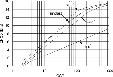
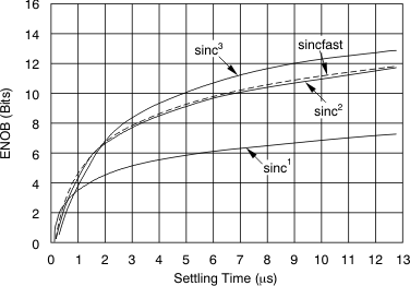
In motor control applications, a very fast response time for overcurrent detection is required. The time for fully settling the filter in case of a step-signal at the input of the modulator depends on its order; that is, a sinc3 filter requires three data updates for full settling (with fDATA = fCLK / OSR). Therefore, for overcurrent protection, filter types other than sinc3 might be better choices. An alternative is, for example, the sinc2 filter. Figure 52 compares the settling times of different filter orders.
Sincfast is a modified sinc2 filter whose transfer function follows Equation 3.


In the case of a continuous signal fed into a sinc filter, the time delay for such signal corresponds to half of the settling time shown in Figure 52.