SBAS654G June 2014 – January 2020 AMC1305L25 , AMC1305M05 , AMC1305M25
PRODUCTION DATA.
- 1 Features
- 2 Applications
- 3 Description
- 4 Revision History
- 5 Device Comparison Table
- 6 Pin Configuration and Functions
-
7 Specifications
- 7.1 Absolute Maximum Ratings
- 7.2 ESD Ratings
- 7.3 Recommended Operating Conditions
- 7.4 Thermal Information
- 7.5 Power Ratings
- 7.6 Insulation Specifications
- 7.7 Safety-Related Certifications
- 7.8 Safety Limiting Values
- 7.9 Electrical Characteristics: AMC1305M05
- 7.10 Electrical Characteristics: AMC1305x25
- 7.11 Switching Characteristics
- 7.12 Insulation Characteristics Curves
- 7.13 Typical Characteristics
- 8 Detailed Description
- 9 Application and Implementation
- 10Power Supply Recommendations
- 11Layout
- 12Device and Documentation Support
- 13Mechanical, Packaging, and Orderable Information
Package Options
Mechanical Data (Package|Pins)
- DW|16
Thermal pad, mechanical data (Package|Pins)
- DW|16
Orderable Information
8.4.1 Fail-Safe Output
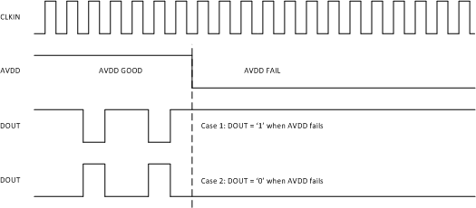
In the case of a missing high-side supply voltage (AVDD), the output of a ΔΣ modulator is not defined and could cause a system malfunction. In systems with high safety requirements, this behavior is not acceptable. Therefore, the AMC1305 implements a fail-safe output function that ensures the device maintains its output level in case of a missing AVDD, as shown in Figure 51.
 Figure 51. Fail-Safe Output of the AMC1305