SLAS836 March 2014 AMC7832
PRODUCTION DATA.
- 1 Features
- 2 Applications
- 3 Description
- 4 Power Amp Biasing Diagram
- 5 Revision History
- 6 Terminal Configuration and Functions
-
7 Specifications
- 7.1 Absolute Maximum Ratings
- 7.2 Handling Ratings
- 7.3 Recommended Operating Conditions
- 7.4 Thermal Information
- 7.5 Electrical Characteristics
- 7.6 Timing Requirements - Serial Interface
- 7.7 Typical Characteristics: DAC
- 7.8 Typical Characteristics: ADC
- 7.9 Typical Characteristics: Reference
- 7.10 Typical Characteristics: Temperature Sensor
-
8 Detailed Description
- 8.1 Overview
- 8.2 Functional Block Diagram
- 8.3 Feature Description
- 8.4 Programming
- 8.5
Register Map
- 8.5.1 Interface Configuration: Address 0x00 - 0x02
- 8.5.2 Device Identification: Address 0x03 - 0x0D
- 8.5.3 Register Update (Buffered Registers): Address 0x0F
- 8.5.4 General Device Configuration: Address 0x10 - 0x17
- 8.5.5 DAC Clear And ALARMOUT Source Select: Address 0x1A - 0x1D
- 8.5.6 DAC Range: Address 0x1E
- 8.5.7 ADC Data: Address 0x20 - 0x41
- 8.5.8 DAC Data: Address 0x50 - 0x67
- 8.5.9 Status Registers: Address 0x70 - 0x72
- 8.5.10 Temperature And GPIO Data: Address 0x78 - 0x7A
- 8.5.11 Out-Of-Range ADC Thresholds: Address 0x80 - 0x93
- 8.5.12 Hysteresis: Address 0xA0 - 0xA5
- 8.5.13 Power-Down Registers: Address 0xB0 - 0xB3
- 8.5.14 ADC Trigger: Address 0xC0
- 9 Applications and Implementation
- 10Power Supply Recommendations
- 11Layout
- 12Device and Documentation Support
- 13Mechanical, Packaging, and Orderable Information
Package Options
Mechanical Data (Package|Pins)
- PAP|64
Thermal pad, mechanical data (Package|Pins)
- PAP|64
Orderable Information
7 Specifications
7.1 Absolute Maximum Ratings
over operating free-air temperature range (unless otherwise noted)(1)| MIN | MAX | UNIT | ||
|---|---|---|---|---|
| Supply voltage range | AVDD to GND | -0.3 | +6 | V |
| DVDD to GND | -0.3 | +6 | V | |
| IOVDD to GND | -0.3 | DVDD | V | |
| AVCC to GND | -0.3 | +18 | V | |
| AVEE to GND | -13 | +0.3 | V | |
| AVSSA,B,C,D to AVEE | -0.3 | +13 | V | |
| AVCC to AVSSA,B,C,D | -0.3 | +26 | V | |
| AVCC to AVEE | -0.3 | +26 | V | |
| DGND to AGND | -0.3 | +0.3 | V | |
| Terminal voltage/ Current range |
ADC_[0-11] analog input voltage to GND | –13 | +13 | V |
| ADC_[0-11] analog input current | -10 | +10 | mA | |
| LV_ADC[12-16] analog input voltage to GND | -0.3 | AVDD + 0.3 | V | |
| LV_ADC[12-16] analog input current | -10 | +10 | mA | |
| DAC outputs to GND | AVSS - 0.3 | AVCC + 0.3 | V | |
| REF_CMP to GND | -0.3 | AVDD + 0.3 | V | |
| REF_OUT[1-2] to GND | -0.3 | AVDD + 0.3 | V | |
| VRANGE[A-D] to GND | -0.3 | AVDD + 0.3 | V | |
| CS, SCLK, SDI and RESET to GND | -0.3 | IOVDD + 0.3 | V | |
| SDO to GND | -0.3 | IOVDD + 0.3 | V | |
| GPIO[0-7] to GND | -0.3 | IOVDD + 0.3 | V | |
| GPIO[0-7] sinking current | 5 | mA | ||
| Operating temperature range | -40 | +125 | °C | |
| Junction temperature range (TJ max) | -40 | +150 | °C | |
(1) Stresses beyond those listed under Absolute Maximum Ratings may cause permanent damage to the device. These are stress ratings only, which do not imply functional operation of the device at these or any other conditions beyond those indicated under Recommended Operating Conditions. Exposure to absolute-maximum-rated conditions for extended periods may affect device reliability.
7.2 Handling Ratings
| PARAMETER | DEFINITION | MIN | MAX | UNIT |
|---|---|---|---|---|
| Tstg | Storage temperature range | -40 | +150 | °C |
| VESD(1) | Human body model (HBM) ESD stress voltage(2) | 2.0 | kV | |
| Charged device model (CDM) ESD stress voltage(3) | 750 | V |
(1) Electrostatic discharge (ESD) to measure device sensitivity and immunity to damage caused by assembly line electrostatic discharges in to the device.
(2) Level listed above is the passing level per ANSI, ESDA, and JEDEC JS-001. JEDEC document JEP155 states that 500-V HBM allows safe manufacturing with a standard ESD control process.
(3) Level listed above is the passing level per EIA-JEDEC JESD22-C101. JEDEC document JEP157 states that 250-V CDM allows safe manufacturing with a standard ESD control process.
7.3 Recommended Operating Conditions
over operating free-air temperature range (unless otherwise noted)| MIN | NOM | MAX | UNIT | |||
|---|---|---|---|---|---|---|
| Supply voltage | AVDD | 4.5 | 5 | 5.5 | V | |
| DVDD (DVDD must be equal to AVDD) | 4.5 | 5 | 5.5 | V | ||
| IOVDD (IOVDD must be equal or less than DVDD) | 1.8 | 5.5 | V | |||
| AVCC | 4.5 | 12 | 12.5 | V | ||
| AVEE | –12.5 | –12 | 0 | V | ||
| AVSSA,B,C,D | AVEE | 0 | V | |||
| Specified temperature range | –40 | 25 | 105 | °C | ||
| Operating temperature range | –40 | 25 | 125 | °C | ||
7.4 Thermal Information
| THERMAL METRIC(1) | AMC7832 | UNIT | |
|---|---|---|---|
| PAP (64 TERMINALS) | |||
| θJA | Junction-to-ambient thermal resistance | 26.5 | °C/W |
| θJCtop | Junction-to-case (top) thermal resistance | 7.9 | |
| θJB | Junction-to-board thermal resistance | 9.9 | |
| ψJT | Junction-to-top characterization parameter | 0.2 | |
| ψJB | Junction-to-board characterization parameter | 9.8 | |
| θJCbot | Junction-to-case (bottom) thermal resistance | 0.3 | |
(1) For more information about traditional and new thermal metrics, see the IC Package Thermal Metrics application report, SPRA953.
7.5 Electrical Characteristics
The electrical ratings specified in this section apply to all specifications in this document, unless otherwise noted. These specifications are interpreted as conditions that do not degrade the device parametric or functional specifications for the life of the product containing it. AVDD = DVDD = +4.5 to +5.5-V, AVCC = +12-V, AVEE = -12-V, IOVDD = +1.8 to +5.5-V, AGND = DGND = 0-V, AVSSA,B,C,D = 0-V (DAC groups in positive ranges) or -12-V (DAC groups in negative range), DAC output range = 0 to 10-V for all groups, no load on the DACs, TA = -40°C to +105°C (unless otherwise noted)| PARAMETER | TEST CONDITIONS | MIN | TYP | MAX | UNIT | |||
|---|---|---|---|---|---|---|---|---|
| DAC SPECIFICATIONS | ||||||||
| DAC DC ACCURACY | ||||||||
| Resolution | 12 | Bits | ||||||
| INL | Relative accuracy | Measured by line passing through codes 020h and FFFh. 0 to +10-V and -10 to 0-V ranges |
±1 | LSB | ||||
| Measured by line passing through codes 040h and FFFh. 0 to +5-V range |
±1.5 | |||||||
| DNL | Differential nonlinearity | Specified monotonic. Measured by line passing through codes 020h and FFFh. 0 to +10-V and -10 to 0-V ranges. Measured by line passing through codes 040h and FFFh. 0 to +5-V range |
±0.3 | ±1 | LSB | |||
| TUE | Total unadjusted error(2) | TA = 25°C 0 to +10-V range and -10 to 0-V ranges |
±20 | mV | ||||
| TA = 25°C 0 to +5-V range |
±10 | mV | ||||||
| Offset error | TA = 25°C, Measured by line passing through codes 020h and FFFh, 0 to +10-V range |
±5 | mV | |||||
| TA = 25°C, Measured by line passing through codes 040h and FFFh, 0 to +5-V range |
±5 | mV | ||||||
| Zero-code error | TA = 25°C, Code 000h, -10 to 0-V range | ±20 | mV | |||||
| Gain error(2) | TA = 25°C, Measured by line passing through codes 020h and FFFh, 0 to +10-V and -10 to 0-V ranges |
±0.2 | %FSR | |||||
| TA = 25°C, Measured by line passing through codes 040h and FFFh, 0 to +5-V range |
±0.2 | %FSR | ||||||
| Offset temperature coefficient | 0 to +10-V and 0 to +5-V ranges | ±1 | ppm/°C | |||||
| Zero-code temperature coefficient | -10 to 0-V range | ±2 | ppm/°C | |||||
| Gain temperature coefficient | All output ranges | ±1 | ppm/°C | |||||
| DAC OUTPUT CHARACTERISTICS | ||||||||
| Full-scale output voltage range(1) | VRANGEn terminal set to AGND DAC-5VRANGEn bit set to 0 |
0 | 10 | V | ||||
| VRANGEn terminal set to AGND DAC-5VRANGEn bit set to 1 |
0 | 5 | V | |||||
| VRANGEn terminal set to +2.5V DAC-5VRANGEn bit set to 0 |
–10 | 0 | V | |||||
| Output voltage settling time | Transition: Code 400h to C00h to within ½ LSB, RL = 2kΩ, CL = 200pF, 0 to +10-V and -10 to 0-V ranges |
10 | µs | |||||
| Transition: Code 400h to C00h to within ½ LSB, RL = 2kΩ, CL = 200pF, 0 to +5-V range |
8 | µs | ||||||
| Slew rate | Transition: Code 400h to C00h to within ½ LSB, RL = 2kΩ, CL = 200pF, all DAC output ranges |
1.25 | V/µs | |||||
| Short-circuit current | Full-scale current shorted to AVSS or AVCC | 45 | mA | |||||
| Load current | Source and/or sink with 1V headroom from AVCC/AVSS, voltage drop < 25mV(4) | ±15 | mA | |||||
| Source and/or sink with 300mV headroom from AVCC/AVSS, voltage drop < 25mV | ±10 | mA | ||||||
| Source with 100mV headroom from AVCC(5) | 0 | mA | ||||||
| Maximum capacitive load(3) | RL = ∞ | 0 | 10 | nF | ||||
| DC output impedance | Code set to 800h, ±15mA | 1 | Ω | |||||
| Power-on overshoot | AVEE = AVSSA,B,C,D = GND, AVCC = 0 to +12V, 2ms ramp |
50 | mV | |||||
| Glitch energy | Transition: Code 7FFh to 800h; 800h to 7FFh | 1 | nV-s | |||||
| Output noise | TA = 25°C, 1kHz, code 800h, includes internal reference noise | 520 | nV/√Hz | |||||
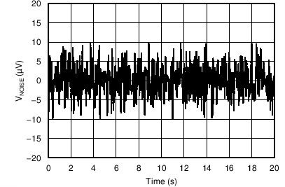
| TA = 25°C, integrated noise from 0.1Hz to 10Hz, code 800h, includes internal reference noise | 20 | µVPP | ||||||
| CLAMP OUTPUTS | ||||||||
| Clamp output voltage(8) | DAC output range: 0 to +10-V | 0 | V | |||||
| DAC output range: 0 to +5-V | 0 | V | ||||||
| DAC output range: -10 to 0-V, AVSS = -12-V |
AVSS + 2 | V | ||||||
| ADC AND TEMPERATURE SENSOR SPECIFICATIONS | ||||||||
| Resolution | 12 | Bits | ||||||
| INL | Integral nonlinearity | Unipolar input channels | ±0.5 | ±1 | LSB | |||
| Bipolar input channels | ±0.75 | ±1.5 | LSB | |||||
| DNL | Differential nonlinearity | Specified monotonic. All input channels | ±0.5 | ±1 | LSB | |||
| UNIPOLAR ANALOG INPUTS: LV_ADC12 to LV_ADC16 | ||||||||
| Absolute input voltage range | GND – 0.2 | AVDD + 0.2 | V | |||||
| Full scale input range | 0 | 2 × VREF | V | |||||
| Input capacitance | VREF measured at REF_CMP terminal | 34 | pF | |||||
| DC input leakage current | Unselected ADC input | ±10 | µA | |||||
| Offset error | ±2 | ±5 | LSB | |||||
| Offset error match | ±2.5 | LSB | ||||||
| Gain error(2) | ±1 | ±5 | LSB | |||||
| Gain error match | ±1 | LSB | ||||||
| Update time | Single unipolar input, temperature sensor disabled | 11.5 | µs | |||||
| BIPOLAR ANALOG INPUTS: ADC_0 to ADC_11 | ||||||||
| Absolute input voltage range | –13 | +13 | V | |||||
| Full scale input range | -12.5 | 12.5 | V | |||||
| Input resistance | 175 | kΩ | ||||||
| Offset error | ±5 | ±10 | LSB | |||||
| Gain error(2) | ±5 | ±10 | LSB | |||||
| Update time | Single bipolar input, temperature sensor disabled | 34.5 | µs | |||||
| TEMPERATURE SENSOR | ||||||||
| Operating range | -40 | 125 | °C | |||||
| Accuracy | TA = -40°C to 125°C, AVDD = +5-V | ±1.25 | ±2.5 | °C | ||||
| Resolution | LSB size | 0.25 | °C | |||||
| Update time | All ADC input channels disabled | 256 | µs | |||||
| AUTOCYCLE UPDATE TIME | ||||||||
| Autocycle update time | All 17 ADC inputs enabled, temperature sensor disabled | 471.5 | µs | |||||
| All 17 ADC inputs and temperature sensor enabled | 727.5 | µs | ||||||
| INTERNAL REFERENCE SPECIFICATIONS | ||||||||
| INTERNAL REFERENCE (Internal reference not accessable) | ||||||||
| Initial accuracy | TA = 25°C | 2.4925 | 2.5 | 2.5075 | V | |||
| Reference temp. coefficient(6) | 12 | 35 | ppm/°C | |||||
| REF_OUT[1-2] BUFFERS(7) | ||||||||
| Reference buffer offset | TA = 25°C | ±2.5 | mV | |||||
| Capacitive load stability | 100 | pF | ||||||
| INTERNAL ADC REFERENCE BUFFER | ||||||||
| Reference buffer offset | TA = 25°C | ±5 | mV | |||||
| GENERAL SPECIFICATIONS | ||||||||
| DIGITAL LOGIC: GPIO | ||||||||
| VIH | High-level input voltage | IOVDD =+1.8 to +5.5-V | 0.7×IOVDD | V | ||||
| VIL | Low-level input voltage | IOVDD = +1.8-V | 0.45 | V | ||||
| IOVDD = +2.7 to +5.5-V | 0.3×IOVDD | V | ||||||
| VOL | Low-level output voltage | IOVDD = +1.8-V, Iload = -2-mA | 0.4 | V | ||||
| IOVDD= +5.5-V, Iload = -5-mA | 0.4 | V | ||||||
| Input impedance | To IOVDD | 48 | kΩ | |||||
| DIGITAL LOGIC: All Except GPIO | ||||||||
| VIH | High-level input voltage | IOVDD = +1.8 to +5.5-V | 0.7×IOVDD | V | ||||
| VIL | Low-level input voltage | IOVDD = +1.8-V | 0.45 | V | ||||
| IOVDD = +2.7 to +5.5-V | 0.3×IOVDD | V | ||||||
| VOH | High-level output voltage | Iload = -1-mA | IOVDD-0.4 | V | ||||
| VOL | Low-level output voltage | Iload = +1-mA | 0.4 | V | ||||
| High-impedance leakage | ±5 | µA | ||||||
| High-impedance output capacitance | 10 | pF | ||||||
| TIMING REQUIREMENTS | ||||||||
| Reset delay | Delay to normal operation from reset | 100 | 250 | µs | ||||
| Power-down recovery time | 70 | µs | ||||||
| Clamp shutdown delay | CL = 10nF | 100 | µs | |||||
| Convert pulse width | 20 | ns | ||||||
| Reset pulse width | 20 | ns | ||||||
| POWER-SUPPLY REQUIREMENTS | ||||||||
| IAVDD | AVDD supply current | No DAC load, all DACs at 800h code and ADC at the fastest auto conversion rate | 10 | mA | ||||
| IAVCC | AVCC supply current | 10 | mA | |||||
| IAVSS | AVSS supply current | –10 | mA | |||||
| IDVDD | DVDD supply current | 3 | mA | |||||
| IIOVDD | IOVDD supply current | 15 | µA | |||||
| Power consumption | 160 | mW | ||||||
| IAVDD | AVDD supply current | Power down mode | 2 | mA | ||||
| IAVCC | AVCC supply current | 2 | mA | |||||
| IAVSS | AVSS supply current | –5.5 | mA | |||||
| IDVDD | DVDD supply current | 2 | mA | |||||
| IIOVDD | IOVDD supply current | 12 | µA | |||||
| Power consumption | 55 | mW | ||||||
(1) The output voltage cannot be greater than AVCC or lower than AVSS. See the DAC Output Range Selection section for more details.
(2) Internal reference contribution not included.
(3) To be sampled during initial release to ensure compliance; not subject to production testing.
(4) If all channels are loaded with 15mA simultaneously care must be taken to ensure the thermal conditions for the device are not exceeded.
(5) Not tested during production. Specified by design.
(6) Not tested during production. Specified by design and characterization.
(7) Intended to drive the VRANGEA,B,C,D inputs only. An external buffer amplifier with high impedance input is required to drive any additional external load.
(8) No DAC load to AVSS.
7.6 Timing Requirements - Serial Interface(1)(2)
AVDD = DVDD = +4.5 to +5.5-V, AVCC = +12-V, AVEE = -12-V, AGND = DGND = AVSSA,B,C,D = 0-V, DAC output range = 0 to +10-V for all groups, no load on the DACs, TA = -40°C to +105°C (unless otherwise noted)| PARAMETER | TEST CONDITIONS | MIN | TYP | MAX | UNIT | |
|---|---|---|---|---|---|---|
| IOVDD = +1.8-V to +2.7-V | ||||||
| fSCLK | SCLK frequency | 15 | MHz | |||
| tP | SCLK period | 66.67 | ns | |||
| tPH | SCLK pulse width high | 27 | ns | |||
| tPL | SCLK pulse width low | 27 | ns | |||
| tSU | SDI setup | 10 | ns | |||
| tH | SDI hold | 10 | ns | |||
| tODZ | SDO driven to tri-state | 0 | 15 | ns | ||
| tOZD | SDO tri-state to driven | 0 | 20 | ns | ||
| tOD | SDO output delay | 0 | 20 | ns | ||
| tCSS | CS setup | 5 | ns | |||
| tCSH | CS hold | 20 | ns | |||
| tIAG | Inter-access gap | 10 | ns | |||
| IOVDD = +2.7-V to +5.5-V | ||||||
| fSCLK | SCLK frequency | 20 | MHz | |||
| tP | SCLK period | 50 | ns | |||
| tPH | SCLK pulse width high | 22.5 | ns | |||
| tPL | SCLK pulse width low | 20 | ns | |||
| tSU | SDI setup | 10 | ns | |||
| tH | SDI hold | 10 | ns | |||
| tODZ | SDO driven to tri-state | 0 | 9 | ns | ||
| tOZD | SDO tri-state to driven | 0 | 12 | ns | ||
| tOD | SDO output delay | 0 | 15 | ns | ||
| tCSS | CS setup | 5 | ns | |||
| tCSH | CS hold | 20 | ns | |||
| tIAG | Inter-access gap | 10 | ns | |||
(1) Specified by design and characterization. Not tested during production.
(2) SDO loaded with 10-pF load capacitance for SDO timing specifications.
 Figure 1. Serial Interface Write Timing Diagram
 Figure 2. Serial Interface Read Timing Diagram
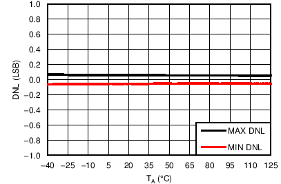
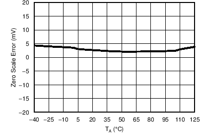
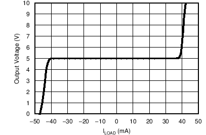
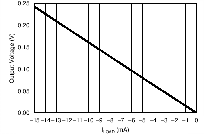
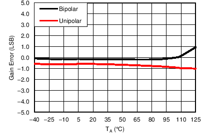
7.7 Typical Characteristics: DAC
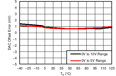
| T = 25°C, 0V to 10V range | ||
| T = 25°C, -10V to 0V range | ||
| T = 25°C, 0V to 5V range | ||
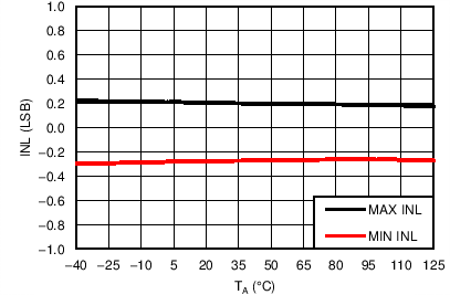
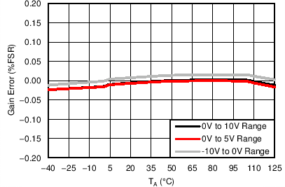
| 0V to 10V range | ||
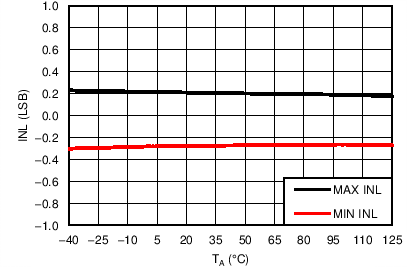
| -10V to 0V range | ||
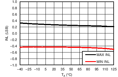
| 0V to 5V range | ||
| T = 25°C, AVCC = 10V, AVEE = 0V, Input Code 0xFFF, 0 to 10V range | ||
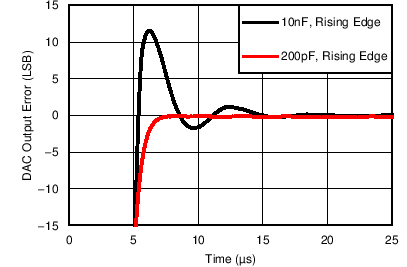
| T = 25°C, Code 0x400 to 0xC00 to within 1/2 LSB | ||
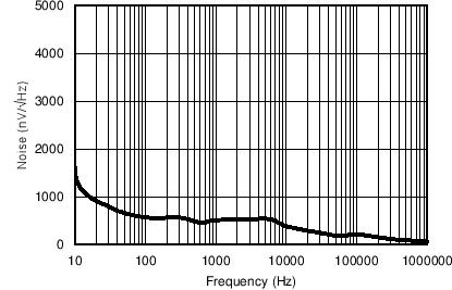
| T = 25°C, Input Code 0x800 | ||
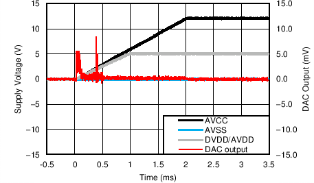
| T = 25°C, AVSS = AVEE = AGND, AVCC 0 to 12V, 2 ms ramp | ||
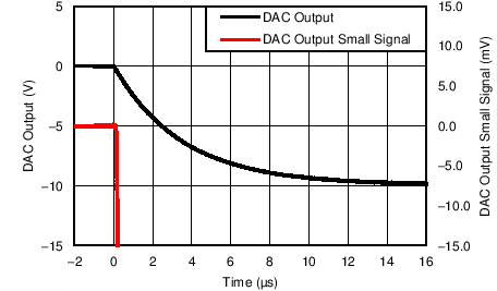
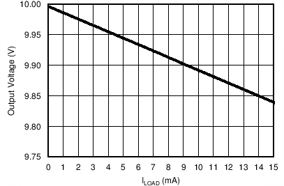
| T = 25°C, -10V to 0V range, DAC Code 0xFFF, No Load | ||
| T = 25°C, -10V to 0V range, DAC Code 0xFFF, No Load | ||
| T = 25°C, 0V to 10V range | ||
| T = 25°C, -10V to 0V range | ||
| T = 25°C, 0V to 5V range | ||
| 0V to 10V range | ||

| -10V to 0V range | ||
| 0V to 5V range | ||
| -10V to 0V range | ||
| T = 25°C, Input Code 0x800, 0 to 10V range | ||
| T = 25°C, AVCC = 10V, AVEE = 0V, Input Code 0x000, 0 to 10V range | ||
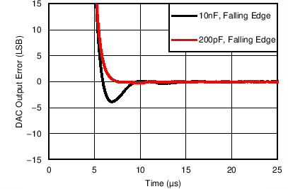
| T = 25°C, Code 0xC00 to 0x400 to within 1/2 LSB | ||
| T = 25°C, Input Code 0x800 | ||
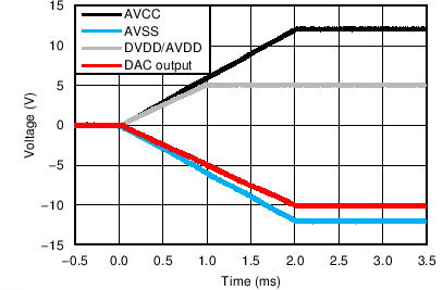
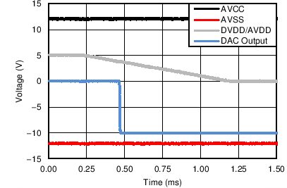
| T = 25°C, AVSS = AVEE = -12V, AVCC 0 to 12V, 2 ms ramp | ||
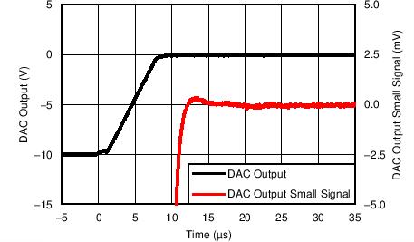
| T = 25°C, -10V to 0V range, DAC Code 0xFFF, No Load | ||
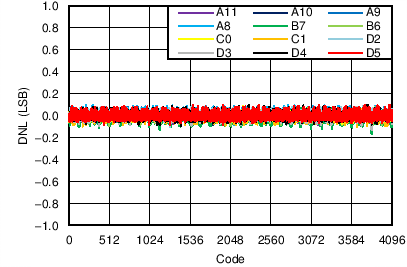
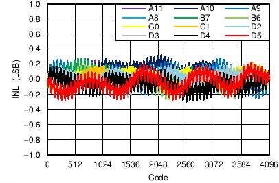
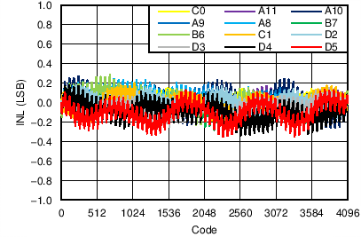
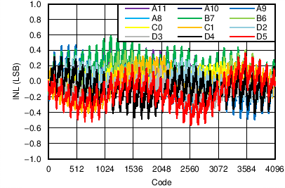
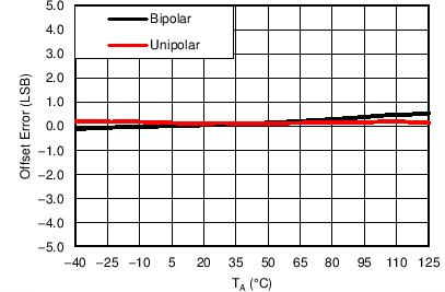
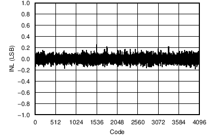
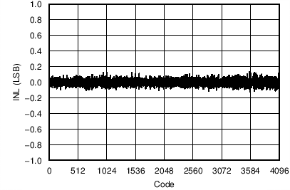
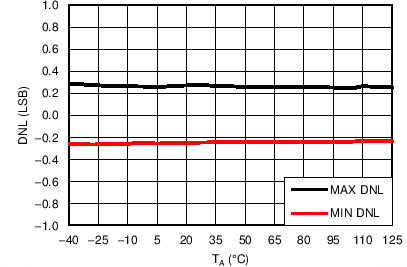
7.8 Typical Characteristics: ADC
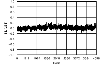
| T = 25°C, Unipolar Input | ||
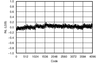
| T = 25°C, Bipolar Input | ||
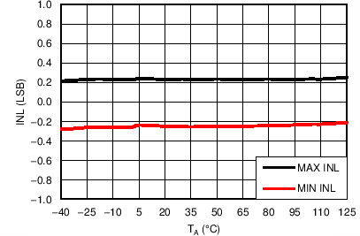
| Unipolar input | ||
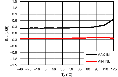
| Bipolar input | ||
| T = 25°C, Unipolar Input | ||
| T = 25°C, Bipolar Input | ||
| Unipolar input | ||
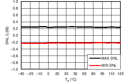
| Bipolar input | ||
7.9 Typical Characteristics: Reference
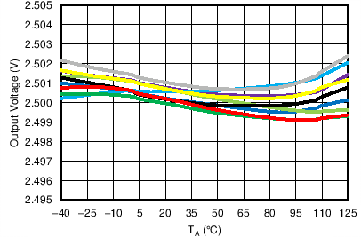
| 10 units, REF_OUT1 | ||
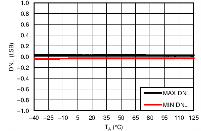
7.10 Typical Characteristics: Temperature Sensor
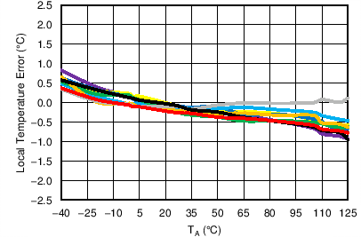
| 10 units | ||