SLAS836 March 2014 AMC7832
PRODUCTION DATA.
- 1 Features
- 2 Applications
- 3 Description
- 4 Power Amp Biasing Diagram
- 5 Revision History
- 6 Terminal Configuration and Functions
-
7 Specifications
- 7.1 Absolute Maximum Ratings
- 7.2 Handling Ratings
- 7.3 Recommended Operating Conditions
- 7.4 Thermal Information
- 7.5 Electrical Characteristics
- 7.6 Timing Requirements - Serial Interface
- 7.7 Typical Characteristics: DAC
- 7.8 Typical Characteristics: ADC
- 7.9 Typical Characteristics: Reference
- 7.10 Typical Characteristics: Temperature Sensor
-
8 Detailed Description
- 8.1 Overview
- 8.2 Functional Block Diagram
- 8.3 Feature Description
- 8.4 Programming
- 8.5
Register Map
- 8.5.1 Interface Configuration: Address 0x00 - 0x02
- 8.5.2 Device Identification: Address 0x03 - 0x0D
- 8.5.3 Register Update (Buffered Registers): Address 0x0F
- 8.5.4 General Device Configuration: Address 0x10 - 0x17
- 8.5.5 DAC Clear And ALARMOUT Source Select: Address 0x1A - 0x1D
- 8.5.6 DAC Range: Address 0x1E
- 8.5.7 ADC Data: Address 0x20 - 0x41
- 8.5.8 DAC Data: Address 0x50 - 0x67
- 8.5.9 Status Registers: Address 0x70 - 0x72
- 8.5.10 Temperature And GPIO Data: Address 0x78 - 0x7A
- 8.5.11 Out-Of-Range ADC Thresholds: Address 0x80 - 0x93
- 8.5.12 Hysteresis: Address 0xA0 - 0xA5
- 8.5.13 Power-Down Registers: Address 0xB0 - 0xB3
- 8.5.14 ADC Trigger: Address 0xC0
- 9 Applications and Implementation
- 10Power Supply Recommendations
- 11Layout
- 12Device and Documentation Support
- 13Mechanical, Packaging, and Orderable Information
Package Options
Mechanical Data (Package|Pins)
- PAP|64
Thermal pad, mechanical data (Package|Pins)
- PAP|64
Orderable Information
6 Terminal Configuration and Functions
HTQFP- 64
PAP Package
(Top View)
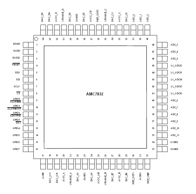
Terminal Functions
| TERMINAL | DESCRIPTION | |
|---|---|---|
| NUMBER | NAME | |
| 1 | DGND | Digital ground. Ground reference point for all digital circuitry on the device. Ideally, AGND and DGND should be at the same potential (GND) and must not differ by more than ±0.3-V. |
| 2 | DVDD | Digital supply voltage. (+4.5-V to +5.5-V). Must be the same value as AVDD. |
| 3 | IOVDD | IO supply voltage. (+1.8-V to +5.5-V). Sets the IO operating voltage and threshold levels. Must not exceed DVDD. |
| 4 | RESET | Reset input, active low. Logic low on this terminal causes the device to perform a hardware reset. |
| 5 | SDO | Serial interface data output. The SDO terminal is in high impedance when CS is high. Data is clocked out of the input shift register on each falling edge of SCLK. |
| 6 | SDI | Serial interface data input. Data is clocked into the input shift register on each rising edge of SCLK. |
| 7 | SCLK | Serial interface clock. |
| 8 | CS | Active low serial data enable. This input is the frame synchronization signal for the serial data. When this signal goes low, it enables the input shift register. |
| 9 | GPIO0/ALARMIN | General purpose digital I/O 0 (default). This terminal is a bidirectional open-drain, digital input/output with internal 48-kΩ pull-up resistor to IOVDD. Alternatively the terminal can be set to operate as ALARMIN, an alarm control signal, digital input, active low. |
| 10 | GPIO1/ ALARMOUT | General purpose digital I/O 1 (default). This terminal is a bidirectional open-drain, digital input/output with internal 48-kΩ pull-up resistor to IOVDD. Alternatively the terminal can be set to operate as ALARMOUT, a global alarm. Open drain output. This terminal goes low (active) when an alarm event is detected. |
| 11 | GPIO2/ADCTRIG | General purpose digital I/O 2 (default). This terminal is a bidirectional open-drain, digital input/output with internal 48-kΩ pull-up resistor to IOVDD. Alternatively the terminal can be set to operate as ADCTRIG, an external conversion trigger, active low. The falling edge starts the sampling and conversion of the ADC. |
| 12 | GPIO3/DAV | General purpose digital I/O 3 (default). This terminal is a bidirectional open-drain, digital input/output with internal 48-kΩ pull-up resistor to IOVDD. Alternatively the terminal can be set to operate as DAV, Data available indicator, active low output. In direct mode, the DAV terminal goes low (active) when the conversion ends. In auto mode, a 1µs pulse (active low) appears on this terminal when a conversion cycle finishes. DAV stays high when deactivated. |
| 13 | GPIO-4 | General purpose digital I/O. This terminal is a bidirectional open-drain, digital input/output with internal 48-kΩ pull-up resistor to IOVDD. |
| 14 | GPIO-5 | |
| 15 | GPIO-6 | |
| 16 | GPIO-7 | |
| 17 | AVEE | Lowest potential in the system. Typically tied to -12-V but if all DACs are set in a positive output range it should be connected to AGND. |
| 18,19, 22, 24 | DAC_A11, DAC_A10, DAC_A9, DAC_A8 |
DAC group A. These channels share the same range and clamp voltage. |
| 20 | AVSSA | Negative analog supply for DAC group A. Sets the power-on-reset and clamp voltage values. Typically tied to AVEE when the DAC range for group A is set to -10 to 0-V or AGND for the positive output ranges. |
| 21 | VRANGEA | This terminal determines the DAC range for DAC group A. If tied to AGND the DAC range is 0 to +5-V or 0 to+10-V. Otherwise if tied to +2.5-V (can be tied to REF_OUT terminals) the DAC range is -10 to 0-V. |
| 23 | AGND1 | Analog ground. Ground reference point for all analog circuitry on the device, AGND. Connect AGND1, AGND2 and AGND3 to the same potential, AGND. |
| 25 | AVCC_AB | Positive analog power for DAC groups A and B. Must be tied to AVCC_CD. |
| 26 | VRANGEB | This terminal determines the DAC range for DAC group B. If tied to AGND the DAC range is 0 to +5-V or 0 to +10-V. Otherwise if tied to +2.5-V (can be tied to REF_OUT terminals) the DAC range is -10 to 0-V. |
| 27, 29 | DAC_B7, DAC_B6 |
DAC group B. These channels share the same range and clamp voltage. |
| 28 | AVSSB | Negative analog supply for DAC group B. Sets the power-on-reset and clamp voltage values. Typically tied to AVEE when the DAC range for group B is set to -10 to 0-V or AGND for the positive output ranges. |
| 30 | REF_OUT1 | Reference output 1. Can be used to drive the VRANGE inputs. |
| 31 | AVDD1 | Analog supply voltage. (+4.5-V to +5.5-V) |
| 32 | REF_CMP | Internal reference compensation capacitor connection (connect 4.7-μF capacitor between this terminal and AGND2). |
| 33 | AGND2 | Analog ground. Ground reference point for all analog circuitry on the device, AGND. Connect AGND1, AGND2 and AGND3 to the same potential, AGND. |
| 34 | AVDD2 | Analog supply voltage. (+4.5-V to +5.5-V) |
| 35-38 | ADC_11, ADC_10, ADC_9, ADC_8 |
Bipolar analog inputs. Typically used to monitor the DAC_A8 to DAC_A11 outputs. The input range of these channels is -12.5-V to +12.5-V. |
| 39-40 | ADC_7, ADC_6 |
Bipolar analog inputs. Typically used to monitor the DAC_B6 to DAC_B7 outputs. The input range of these channels is -12.5-V to +12.5-V. |
| 41-45 | LV_ADC16 to LV_ADC12 | Unipolar analog inputs. These channels are used for general monitoring and their input range is 0 to 2 x VREF. |
| 46-49 | ADC_5, ADC_4, ADC_3, ADC_2 |
Bipolar analog inputs. Typically used to monitor the DAC_D2 to DAC_D5 outputs. The input range of these channels is -12.5-V to +12.5-V. |
| 50-51 | ADC_1, ADC_0 |
Bipolar analog inputs. Typically used to monitor the DAC_C0 to DAC_C1 outputs. The input range of these channels is -12.5-V to +12.5-V. |
| 52,54 | DAC_C1, DAC_C0 |
DAC group C. These channels share the same range and clamp voltage. |
| 53 | AVSSC | Negative analog supply for DAC group C. Sets the power-on-reset and clamp voltage values. Typically tied to AVEE when the DAC range for group C is set to -10 to 0-V or AGND for the positive output ranges. |
| 55 | VRANGEC | This terminal determines the DAC range for DAC group C. If tied to AGND the DAC range is 0 to +5-V or 0 to +10-V. Otherwise if tied to +2.5-V (can be tied to REF_OUT terminals) the DAC range is -10 to 0-V. |
| 56 | REF_OUT2 | Reference output 2. Can be used to drive the VRANGE inputs. |
| 57 | AVCC_CD | Positive analog power for DAC groups C and D. Must be tied to AVCC_AB. |
| 58, 60, 63, 64 | DAC_D5, DAC_D4, DAC_D3, DAC_D2 |
DAC group D. These channels share the same range and clamp voltage. |
| 59 | AGND3 | Analog ground. Ground reference point for all analog circuitry on the device, AGND. Connect AGND1, AGND2 and AGND3 to the same potential, AGND. |
| 61 | VRANGED | This terminal determines the DAC range for DAC group D. If tied to AGND the DAC range is 0 to 5-V or 0 to 10-V. Otherwise if tied to +2.5-V (can be tied to REF_OUT terminals) the DAC range is -10 to 0-V. |
| 62 | AVSSD | Negative analog supply for DAC group D. Sets the power-on-reset and clamp voltage values. Typically tied to AVEE when the DAC range for group D is set to -10 to 0-V or AGND for the positive output ranges. |
| — | THERMAL PAD | The thermal pad is located on the package underside. Should be tied to AVEE or left unconnected. |