SLUSCE2D April   2016  – January 2019

PRODUCTION DATA.  

  1. Features
  2. Applications
  3. Description
    1.     Device Images
      1.      Simplified Schematic
  4. Revision History
  5. Device Comparison
  6. Pin Configuration and Functions
    1.     Pin Functions
  7. Specifications
    1. 7.1 Absolute Maximum Ratings
    2. 7.2 ESD Ratings
    3. 7.3 Recommended Operating Conditions
    4. 7.4 Thermal Information
    5. 7.5 Electrical Characteristics
    6. 7.6 Timing Requirements
    7. 7.7 Typical Operational Characteristics (Protection Circuits Waveforms)
  8. Detailed Description
    1. 8.1 Overview
    2. 8.2 Functional Block Diagram
    3. 8.3 Feature Description
      1. 8.3.1 Power-Down or Undervoltage Lockout (UVLO)
      2. 8.3.2 Power-up
      3. 8.3.3 Sleep Mode
      4. 8.3.4 New Charge Cycle
      5. 8.3.5 Overvoltage-Protection (OVP) – Continuously Monitored
      6. 8.3.6 CHG Terminal Indication
    4. 8.4 Device Functional Modes
      1. 8.4.1  CHG LED Pull-up Source
      2. 8.4.2  IN-DPM (VIN-DPM or IN-DPM)
      3. 8.4.3  OUT
      4. 8.4.4  ISET
      5. 8.4.5  TS
      6. 8.4.6  Termination and Timer Disable Mode (TTDM) - TS Terminal High
      7. 8.4.7  Timers
      8. 8.4.8  Termination
      9. 8.4.9  Battery Detect Routine
      10. 8.4.10 Refresh Threshold
      11. 8.4.11 Starting a Charge on a Full Battery
  9. Application and Implementation
    1. 9.1 Application Information
    2. 9.2 Typical Application
      1. 9.2.1 Design Requirements
      2. 9.2.2 Detailed Design Procedure
        1. 9.2.2.1 Calculations
          1. 9.2.2.1.1 Program the Fast Charge Current, ISET:
          2. 9.2.2.1.2 Pre-Charge and Termination Current Thresholds, ITERM, and PRE-CHG
          3. 9.2.2.1.3 TS Function
          4. 9.2.2.1.4 CHG
        2. 9.2.2.2 Selecting In and Out Terminal Capacitors
      3. 9.2.3 Application Curves
  10. 10Power Supply Recommendations
  11. 11Layout
    1. 11.1 Layout Guidelines
    2. 11.2 Layout Example
    3. 11.3 Thermal Considerations
      1. 11.3.1 Leakage Current Effects on Battery Capacity
  12. 12Device and Documentation Support
    1. 12.1 Receiving Notification of Documentation Updates
    2. 12.2 Community Resources
    3. 12.3 Trademarks
    4. 12.4 Electrostatic Discharge Caution
    5. 12.5 Glossary
  13. 13Mechanical, Packaging, and Orderable Information

Package Options

Mechanical Data (Package|Pins)
Thermal pad, mechanical data (Package|Pins)
Orderable Information

New Charge Cycle

A new charge cycle is started when a good power source is applied, performing a chip disable/enable (TS terminal), exiting Termination and Timer Disable Mode (TTDM), detecting a battery insertion or the OUT voltage dropping below the VRCH threshold. The CHG terminal is active low only during the first charge cycle, therefore exiting TTDM or a dropping below VRCH will not turn on the CHG terminal FET, if the CHG terminal is already high impedance.

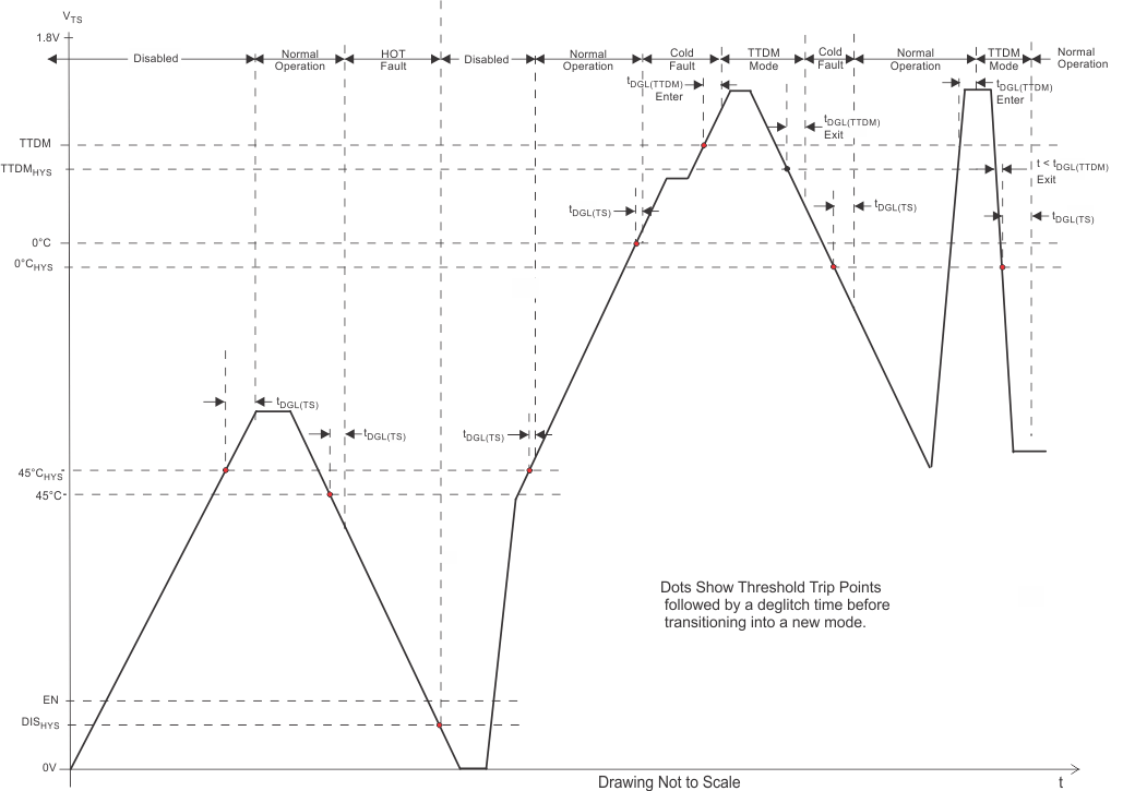
bq21040 batt_temp_slusce2.gifFigure 6. TS Battery Temperature Bias Threshold and Deglitch Timers
bq21040 power-up_flow_slusce2.gifFigure 7. bq21040 Power-Up Flow Diagram