SLUS694G March 2006 – December 2014
PRODUCTION DATA.
- 1 Features
- 2 Applications
- 3 Description
- 4 Revision History
- 5 Device Comparison Table
- 6 Pin Configuration and Functions
- 7 Specifications
-
8 Detailed Description
- 8.1 Overview
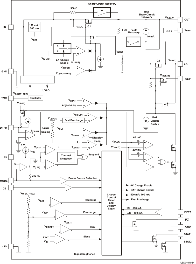
- 8.2 Functional Block Diagram
- 8.3 Feature Description
- 8.4
Device Functional Modes
- 8.4.1 Sleep Mode - V(IN) < VI(BAT)
- 8.4.2 Standy Mode - V(IN) > VI(BAT)and CE (Chip Enable) Pin = Low
- 8.4.3
Battery Charge Mode - V(IN) > VI(BAT), Battery Present, CE pin = High and DPPM Pin Not Floating
- 8.4.3.1 Automous Power Selection and Boot-Up Sequence
- 8.4.3.2 Charge Control
- 8.4.3.3 Battery Preconditioning
- 8.4.3.4 Battery Charge Current
- 8.4.3.5 Battery Voltage Regulation
- 8.4.3.6 Temperature Regulation and Thermal Protection
- 8.4.3.7 Charge Timer Operation
- 8.4.3.8 Timer Fault Recovery
- 8.4.3.9 Charge Termination and Recharge
- 9 Application and Implementation
- 10Power Supply Recommendations
- 11Layout
- 12Device and Documentation Support
- 13Mechanical, Packaging, and Orderable Information
Package Options
Refer to the PDF data sheet for device specific package drawings
Mechanical Data (Package|Pins)
- RHL|20
Thermal pad, mechanical data (Package|Pins)
- RHL|20
Orderable Information
8 Detailed Description
8.1 Overview
The bq2407x device is a highly-integrated Li-ion linear charger and system power-path management device targeted at space-limited portable applications. The bq2407x devices offer DC supply (AC adapter) power-path management with autonomous power-source selection, power FETs and current sensors, high-accuracy current and voltage regulation, charge status, and charge termination, in a single monolithic device.
The bq2407x devices support a precision Li-ion or Li-polymer charging system suitable for single-cell portable devices. See a typical charge profile, application circuits, and an operational flow chart in Figure 2 through Figure 6, respectively.
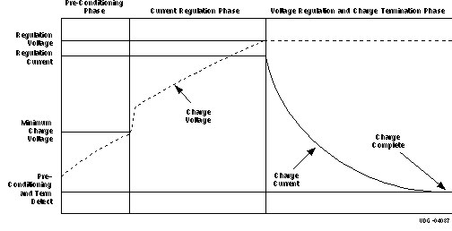 Figure 2. Charge Profile
The bq2407x devices power the system while independently charging the battery. This feature reduces the charge and discharge cycles on the battery, allows for proper charge termination and allows the system to run with an absent or defective battery pack. This feature also allows for the system to instantaneously turn on from an external power source in the case of a deeply discharged battery pack. The IC design is focused on supplying continuous power to the system when available from the AC adapter or battery sources.
8.3 Feature Description
8.3.1 Power-Path Management
The bq2407x devices power the system while independently charging the battery. This feature reduces the charge and discharge cycles on the battery, allows for proper charge termination, and allows the system to run with an absent or defective battery pack. This feature gives the system priority on input power, allowing the system to power up with a deeply discharged battery pack. This feature works as follows:
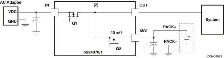 Figure 3. Power-Path Management
8.3.1.1 Case 1: IN Mode (Mode = High)
8.3.1.1.1 System Power
In this case, the system load is powered directly from the AC adapter through the internal transistor Q1 (see Figure 3). The output is regulated at 4.4 V (bq24070). If the system load exceeds the capacity of the supply, the output voltage drops down to the voltage of the battery.
8.3.1.1.2 Charge Control
When in IN mode, the battery is charged through switch Q2 based on the charge rate set on the ISET1 input.
8.3.1.1.3 Dynamic Power-Path Management (DPPM)
This feature monitors the output voltage (system voltage) for input power loss due to brown outs, current limiting, or removal of the input supply. If the voltage on the OUT pin drops to a preset value, V(DPPM) × SF, due to a limited amount of input current, then the battery charging current is reduced until the output voltage stops dropping. The DPPM control tries to reach a steady-state condition where the system gets its needed current and the battery is charged with the remaining current. No active control limits the current to the system; therefore, if the system demands more current than the input can provide, the output voltage drops just below the battery voltage and Q2 turns on which supplements the input current to the system. DPPM has three main advantages.
- This feature allows the designer to select a lower power wall adapter, if the average system load is moderate compared to its peak power. For example, if the peak system load is 1.75 A, average system load is 0.5 A and battery fast-charge current is 1.25 A, the total peak demand could be 3 A. With DPPM, a 2-A adaptor could be selected instead of a 3.25-A supply. During the system peak load of 1.75 A and charge load of 1.25 A, the smaller adaptor’s voltage drops until the output voltage reaches the DPPM regulation voltage threshold. The charge current is reduced until there is no further drop on the output voltage. The system gets its 1.75-A charge and the battery charge current is reduced from 1.25 A to 0.25 A. When the peak system load drops to 0.5 A, the charge current returns to 1 A and the output voltage returns to its normal value.
- Using DPPM provides a power savings compared to configurations without DPPM. Without DPPM, if the system current plus charge current exceed the supply’s current limit, then the output is pulled down to the battery. Linear chargers dissipate the unused power (VIN-VOUT) × ILOAD. The current remains high (at current limit) and the voltage drop is large for maximum power dissipation. With DPPM, the voltage drop is less (VIN-V(DPPM-REG)) to the system which means better efficiency. The efficiency for charging the battery is the same for both cases. The advantages include less power dissipation, lower system temperature, and better overall efficiency.
- If possible, the DPPM sustains the system voltage no matter what causes it to drop. The DPPM does this by reducing the noncritical charging load while maintaining the maximum power output of the adaptor.
The DPPM voltage, V(DPPM), is programmed as follows:

where
- R(DPPM) is the external resistor connected between the DPPM and VSS pins
- I(DPPM) is the internal current source
- SF is the scale factor as specified in the specification table
The safety timer is dynamically adjusted while in DPPM mode. The voltage on the ISET1 pin is directly proportional to the programmed charging current. When the programmed charging current is reduced, due to DPPM, the ISET1 and TMR voltages are reduced and the timer clock is proportionally slowed, extending the safety time. In normal operation V(TMR) = 2.5 V; and, when the clock is slowed, V(TMR) is reduced. When V(TMR) = 1.25 V, the safety timer has a value close to 2 times the normal operation timer value. See Figure 10 through Figure 9.
8.3.1.2 Case 2: USB Mode (Mode = L)
8.3.1.2.1 System Power
In this case, the system load is powered from a USB port through the internal switch Q1 (see Figure 3). In this case, Q1 regulates the total current to the 100-mA or 500-mA level, as selected on the ISET2 input. The output, VOUT, is regulated to 4.4 V (bq24070). The power management of the system is responsible for keeping its system load below the USB current level selected (if the battery is critically low or missing). Otherwise, the output drops to the battery voltage; therefore, the system should have a low-power mode for USB power application. The DPPM feature keeps the output from dropping below its programmed threshold, due to the battery charging current, by reducing the charging current.
8.3.1.2.2 Charge Control
When in USB mode, Q1 regulates the input current to the value selected by the ISET2 pin (0.1/0.5 A). The charge current to the battery is set by the ISET1 resistor (typically > 0.5 A). Because the charge current typically is programmed for more current than the USB current limit allows, the output voltage drops to the battery voltage or DPPM voltage, whichever is higher. If the DPPM threshold is reached first, the charge current is reduced until VOUT stops dropping. If VOUT drops to the battery voltage, the battery is able to supplement the input current to the system.
8.3.1.2.3 Dynamic Power-Path Management (DPPM)
The theory of operation is the same as described in CASE 1, except that Q1 is restricted to the USB current level selected by the ISET2 pin.
The DPPM voltage, V(DPPM), is programmed as follows:
where
- R(DPPM) is the external resistor connected between the DPPM and VSS pins
- I(DPPM) is the internal current source
- SF is the scale factor as specified in the specification table
8.3.1.2.4 Application Curve Descriptions
Refer to the applications section to view the curves. Figure 10 illustrates DPPM and battery supplement modes as the output current (IOUT) is increased; channel 1 (CH1) VIN (VAC) = 5.4 V; channel 2 (CH2) VOUT; channel 3 (CH3) IOUT = 0 to 2.2 A to 0 A; channel 4 (CH4) VBAT = 3.5 V; I(PGM-CHG) = 1 A. The output load is increased from 0 A to approximately 2.2 A and back to 0 A as shown in the bottom waveform. As the IOUT load reaches 0.5 A, along with the 1-A charge current, the adaptor starts to current limit, the output voltage drops to the DPPM-OUT threshold of 4.26 V. This is DPPM mode. The IN input tracks the output voltage by the dropout voltage of the IN FET. The battery charge current is then adjusted back as necessary to keep the output voltage from falling any further. Once the output load current exceeds the input current, the battery has to supplement the excess current and the output voltage falls just below the battery voltage by the dropout voltage of the battery FET. This is the battery supplement mode. When the output load current is reduced, the operation described is reversed as shown. If the DPPM-OUT voltage was set below the battery voltage, during input current limiting, the output falls directly to the battery's voltage.
Under USB operation, when the loads exceeds the programmed input current thresholds a similar pattern is observed. If the output load exceeds the available USB current, the output instantly goes into the battery supplement mode.
Figure 8 illustrates when a battery is inserted for power up; channel 1 (CH1) VIN = 0 V; channel 2 (CH2) VUSB = 0 V; channel 3 (CH3) VOUT; output current, IOUT = 0.25 A for VOUT > 2 V; channel 4 (CH4) VBAT = 3.5 V; C(DPPM) = 0 pF. When there are no power sources and the battery is inserted, the output tracks the battery voltage if there is no load (<10 mA of load) on the output, as shown. If a load is present that keeps the output more than 200 mV below the battery, a short-circuit condition is declared. At this time, the load has to be removed to recover. A capacitor can be placed on the DPPM pin to delay implementing the short-circuit mode and get unrestricted (not limited) current.
Figure 9 illustrates USB boot up and power-up through USB; channel 1 (CH1) V(IN) (VAC) = 0 to 5 V; channel 2 (CH2) IN input current (0.2 A/div); Mode = Low; CE = High; ISET2 = High; VBAT = 3.85 V; V(DPPM) = 3.0 V (V(DPPM) × 1.15 < VBAT, otherwise DPPM mode increases time duration). When a USB source is applied (if IN is not present), the CE pin and ISET2 pin are ignored during the boot-up time and a maximum input current of 100 mA is made available to the OUT or BAT pins. After the boot-up time, the IC implements the CE and ISET2 pins as programmed.
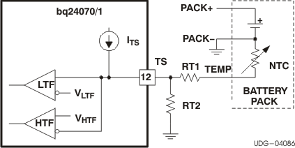
8.3.2 Battery Temperature Monitoring
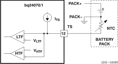
The bq2407x continuously monitors battery temperature by measuring the voltage between the TS and VSS pins. An internal current source provides the bias for most-common 10 kΩ negative-temperature coefficient thermistors (NTC) (see Figure 4). The device compares the voltage on the TS pin against the internal V(LTF) and V(HTF) thresholds to determine if charging is allowed. Once a temperature outside the V(LTF) and V(HTF) thresholds is detected, the device immediately suspends the charge. The device suspends charge by turning off the power FET and holding the timer value (that is, timers are not reset). Charge is resumed when the temperature returns to the normal range. The allowed temperature range for 103AT-type thermistor is 0°C to 45°C. However, the user may increase the range by adding two external resistors. See Figure 5.
8.3.3 Charge Status Outputs
The open-drain (OD) STAT1 and STAT2 outputs indicate various charger operations as shown in Table 1. These status pins can be used to drive LEDs or communicate to the host processor. Note that OFF indicates the open-drain transistor is turned off. Note that OFF assumes CE = High.
Table 1. Status Pins Summary
| CHARGE STATE | STAT1 | STAT2 |
|---|---|---|
| Precharge in progress | ON | ON |
| Fast charge in progress | ON | OFF |
| Charge done | OFF | ON |
| Charge suspend (temperature), timer fault, and sleep mode | OFF | OFF |
8.3.4 PG, Outputs (Power Good)
The open-drain pin, PG, indicates when input power is present, and above the battery voltage. The corresponding output turns ON (low) when exiting sleep mode (input voltage above battery voltage). This output is turned off in the sleep mode (open drain). The PG pin can be used to drive an LED or communicate to the host processor. Note that OFF indicates the open-drain transistor is turned off.
8.3.5 Short-Circuit Recovery
The output can experience two types of short-circuit protection, one associated with the input and one with the battery.
If the output drops below approximately 1 V, an input short-circuit condition is declared and the input FET, Q1 is turned off. To recover from this state, a 500-Ω pullup resistor from the input is applied (switched) to the output. To recover, the load on the output has to be reduced {Rload > 1 V × 500 Ω/ (Vin–Vout)} such that the pullup resistor is able to lift the output voltage above 1 V, for the input FET to be turned back on.
If the output drops 200 mV below the battery voltage, the battery FET, Q2 is considered in short circuit and the battery FET turns off. To recover from this state, there is a 10-mA current source from the battery to the output. Once the output load is reduced, such that the 10-mA current source can pick up the output within 200 mV of the battery, the FET turns back on.
If the short is removed, and the minimum system load is still too large [R<(VBat-200 mV) / 10 mA], the short-circuit protection can be temporarily defeated. The battery short-circuit protection can be disabled (recommended only for a short time) if the voltage on the DPPM pin is less than 1 V. Pulsing this pin below 1 V, for a few microseconds, should be enough to recover.
This short-circuit disable feature was implemented mainly for power up when inserting a battery. Because the BAT input voltage rises much faster than the OUT voltage (Vout<Vbat-200 mV), with most any capacitive load on the output, the part can get stuck in short-circuit mode. Placing a capacitor between the DPPM pin and ground slows the VDPPM rise time, during power up, and delays the short-circuit protection. Too large a capacitance on this pin (too much of a delay) could allow too-high currents if the output was shorted to ground. The recommended capacitance is 1 nF to 10 nF. The VDPPM rise time is a function of the 100-μA DPPM current source, the DPPM resistor, and the capacitor added.
8.3.6 VREF
The VREF is used for internal reference and compensation (3.3 V typ). Additionally, it can be used to disable the safety timer and termination by connecting the TMR to the VREF pin. For internal compensation, the VREF pin requires a minimum 0.1-μF ceramic capacitor. The VREF capacitor should not exceed 1 μF.
8.4 Device Functional Modes
8.4.1 Sleep Mode - V(IN) < VI(BAT)
The bq2407x charger circuitry enters the low-power sleep mode if the input is removed from the circuit. This feature prevents draining the battery into the bq2407x during the absence of input supply. Note that in sleep mode, Q2 remains on (that is, battery connected to the OUT pin) in order for the battery to continue supplying power to the system.
8.4.2 Standy Mode - V(IN) > VI(BAT)and CE (Chip Enable) Pin = Low
The CE (chip enable) digital input is used to disable or enable the IC. A high-level signal on this pin enables the chip, and a low-level signal disables the device and initiates the standby mode. The bq2407x enters the low-power standby mode when the CE input is low with input present. In this suspend mode, internal power FET Q1 (see Figure 3) is turned off; the battery (BAT pin) is used to power the system through Q2 and the OUT pin. This feature is designed to limit the power drawn from the input supply (such as USB suspend mode).
8.4.3 Battery Charge Mode - V(IN) > VI(BAT), Battery Present, CE pin = High and DPPM Pin Not Floating
8.4.3.1 Automous Power Selection and Boot-Up Sequence
The MODE control pin selects the priority of the input sources. If an input source is not available, the battery is selected as the source. With the MODE pin high, the bq2407x charges from the input at the charge rate set by the ISET1 pin. With the MODE pin low, the bq2407x defaults to the USB charging at the charge rate, and the supply current is limited by the ISET2 pin (100 mA for ISET2 = Low, 500 mA for ISET2 = High). This feature allows the use of a single connector (mini-USB cable), where the host programs the MODE pin according to the source that is connected (AC adaptor or USB port). Table 2 summarizes the MODE pin function.
Table 2. Power Source Selection Function Summary
| MODE STATE | AC ADAPTER |
MAXIMUM CHARGE RATE(1) |
SYSTEM POWER SOURCE | USB BOOT-UP FEATURE | ||
|---|---|---|---|---|---|---|
| Low | Present | ISET2 | USB | Enabled | ||
| Absent | N/A | Battery | Disabled | |||
| High | Present | ISET1 | IN | Disabled | ||
| Absent | N/A | Battery | Disabled | |||
With Mode= Low, in order to facilitate the system start-up and USB enumeration, the bq2407x offers a proprietary boot-up sequence. On the first application of power to the bq2407x, this feature enables the 100-mA USB charge rate for a period of approximately 150 ms, (t(BOOT-UP)), ignoring the ISET2 and CE inputs setting. At the end of this period, the bq2407x implement CE and ISET2 input settings. See Figure 9.
V(OUT) is regulated to VO(OUT-REG) as long as the the system load, I(SYS), plus the battery charge current, IO(BAT), set by ISET1 does not exceed the maximum input current of
IIN = 2 A if MODE is high or
IIN set by ISET2 if MODE is low.
If V(OUT) drops to the DPPM pin preset value, V(DPPM) × SF, due to a limited amount of input current, then the battery charging current is dynamically reduced until the output voltage stops dropping. If the system demands more current than the input can provide, the output voltage drops just below the battery voltage and Q2 turns on which allows the battery to supplement the input current to the system. The DPPM circuity is explained in detail in Power-Path Management. The following sections explain the battery charge process in detail. Floating the DPPM pin disables battery charging.
8.4.3.2 Charge Control
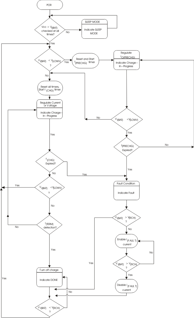 Figure 6. Charge Control Operational Flow Chart
8.4.3.3 Battery Preconditioning
During a charge cycle, if the battery voltage is below the V(LOWV) threshold, the bq2407x applies a precharge current, IO(PRECHG), to the battery. This feature revives deeply discharged cells. The RSET resistor, connected between the ISET1 and VSS pins, determines the precharge rate. The V(PRECHG) and K(SET) parameters are specified in the specifications table. Note that this applies to both IN-mode and USB-mode charging.
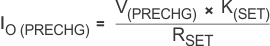
The bq2407x activates a safety timer, t(PRECHG), during the conditioning phase. If V(LOWV) threshold is not reached within the timer period, the bq2407x turns off the charger and enunciates FAULT on the STAT1 and STAT2 pins. The time-out is extended if the charge current is reduced by DPPM or thermal regulation. See the Timer Fault Recovery section for additional details.
8.4.3.4 Battery Charge Current
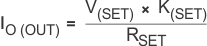
The bq2407x offers on-chip current regulation with programmable set point. The RSET resistor, connected between the ISET1 and VSS pins, determines the charge level. The charge level may be reduced to give the system priority on input current (see DPPM). The V(SET) and K(SET) parameters are specified in the specifications table.
When powered from a USB port, the input current available (0.1 A/0.5 A) is typically less than the programmed (ISET1) charging current, and therefore, the DPPM feature attempts to keep the output from being pulled down by reducing the charging current.
The charge level, during IN mode operation only (Mode = High), can be changed by a factor of 2 by setting the ISET2 pin high (full charge) or low (half charge). The voltage on the ISET1 pin, VSET1, is divided by 2 when in the half constant current charge mode. Note that with Mode low, the ISET2 pin controls only the 0.1 A/0.5 A USB current level.
See Power-Path Management for additional details.
8.4.3.5 Battery Voltage Regulation
The voltage regulation feedback is through the BAT pin. This input is tied directly to the positive side of the battery pack. The bq2407x monitors the battery-pack voltage between the BAT and VSS pins. When the battery voltage rises to the VO(REG) threshold, the voltage regulation phase begins and the charging current begins to taper down.
If the battery is absent, the BAT pin cycles between charge done (VO(REG)) and charging (battery recharge threshold, approximately 4.1 V).
See Figure 8 for power up by battery insertion.
As a safety backup, the bq2407x also monitors the charge time in the charge mode. If charge is not terminated within this time period, t(CHG), the bq2407x turns off the charger and enunciates FAULT on the STAT1 and STAT2 pins. See the DPPM operation under Case 1 for information on extending the safety timer during DPPM operation. See the Timer Fault Recovery section for additional details.
8.4.3.6 Temperature Regulation and Thermal Protection
To maximize charge rate, the bq2407x features a junction temperature regulation loop. If the power dissipation of the IC results in a junction temperature greater than the TJ(REG) threshold, the bq2407x throttles back on the charge current to maintain a junction temperature around the TJ(REG) threshold. To avoid false termination, the termination detect function is disabled while in this mode.
The bq2407x also monitors the junction temperature, TJ, of the die and disconnects the OUT pin from the IN input if TJ exceeds T(SHTDWN). This operation continues until TJ falls below T(SHTDWN) by the hysteresis level specified in the specification table.
The battery supplement mode has no thermal protection. The Q2 FET continues to connect the battery to the output (system), if input power is not sufficient; however, a short-circuit protection circuit limits the battery discharge current such that the maximum power dissipation of the part is not exceeded under typical design conditions.
8.4.3.7 Charge Timer Operation
As a safety backup, the bq2407x monitors the charge time in the charge mode. If the termination threshold is not detected within the time period, t(CHG), the bq2407x turns off the charger and enunciates FAULT on the STAT1 and STAT2 pins. The resistor connected between the TMR and VSS, RTMR, determines the timer period. The K(TMR) parameter is specified in the specifications table. In order to disable the charge timer, eliminate RTMR, connect the TMR pin directly to the VREF pin. Note that this action eliminates the fast-charge safety timer (it does not disable or reset the precharge safety timer), and also clears any timer fault. TMR pin should not be left floating.

While in the thermal regulation mode or DPPM mode, the bq2407x dynamically adjusts the timer period in order to provide the additional time needed to fully charge the battery. This proprietary feature is designed to prevent against early or false termination. The maximum charge time in this mode, t(CHG-TREG), is calculated by Equation 6.
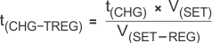
Note that because this adjustment is dynamic and changes as the ambient temperature changes and the charge level changes, the timer clock is adjusted. It is difficult to estimate a total safety time without integrating the above equation over the charge cycle. Therefore, understanding the theory that the safety time is adjusted inversely proportionately with the charge current and the battery is a current-hour rating, the safety time dynamically adjusts appropriately.
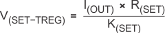
The V(SET) parameter is specified in the specifications table. V(SET-TREG) is the voltage on the ISET pin during the thermal regulation or DPPM mode and is a function of charge current. (Note that charge current is dynamically adjusted during the thermal regulation or DPPM mode.)
All deglitch times also adjusted proportionally to t(CHG-TREG).
8.4.3.8 Timer Fault Recovery
As shown in Figure 6, bq2407x provides a recovery method to deal with timer fault conditions. The following summarizes this method:
Condition 1: Charge voltage above recharge threshold (V(RCH)) and time-out fault occurs.
Recovery Method: bq2407x waits for the battery voltage to fall below the recharge threshold. This could happen as a result of a load on the battery, self-discharge, or battery removal. Once the battery falls below the recharge threshold, the bq2407x clears the fault and starts a new charge cycle. A POR or CE toggle also clears the fault.
Condition 2: Charge voltage below recharge threshold (V(RCH)) and time-out fault occurs.
Recovery Method: Under this scenario, the bq2407x applies the I(FAULT) current. This small current is used to detect a battery removal condition and remains on as long as the battery voltage stays below the recharge threshold. If the battery voltage goes above the recharge threshold, then the bq2407x disables the I(FAULT) current and executes the recovery method described for condition 1. Once the battery falls below the recharge threshold, the bq2407x clears the fault and starts a new charge cycle. A POR or CE toggle also clears the fault.
8.4.3.9 Charge Termination and Recharge
The bq2407x monitors the voltage on the ISET1 pin, during voltage regulation, to determine when termination should occur. Termination occurs when the charge current tapers down to either 1/10th of the programmed fast charge rate (when the MODE pin is high) or 1/25th of the programmed fast charge rate (when the MODE pin is low). Once the termination threshold, I(TERM), is detected the bq2407x terminates charge. The RSET resistor, connected between the ISET1 and VSS pins, programs the fast charge current level and thus the current termination threshold level. The V(TERM) and K(SET) parameters are specified in the specifications table. Note that this applies to both IN and USB charging.

After charge termination, the bq2407x re-starts the charge once the voltage on the BAT pin falls below the V(RCH) threshold. This feature keeps the battery at full capacity at all times.