SLUS694G March 2006 – December 2014
PRODUCTION DATA.
- 1 Features
- 2 Applications
- 3 Description
- 4 Revision History
- 5 Device Comparison Table
- 6 Pin Configuration and Functions
- 7 Specifications
-
8 Detailed Description
- 8.1 Overview
- 8.2 Functional Block Diagram
- 8.3 Feature Description
- 8.4
Device Functional Modes
- 8.4.1 Sleep Mode - V(IN) < VI(BAT)
- 8.4.2 Standy Mode - V(IN) > VI(BAT)and CE (Chip Enable) Pin = Low
- 8.4.3
Battery Charge Mode - V(IN) > VI(BAT), Battery Present, CE pin = High and DPPM Pin Not Floating
- 8.4.3.1 Automous Power Selection and Boot-Up Sequence
- 8.4.3.2 Charge Control
- 8.4.3.3 Battery Preconditioning
- 8.4.3.4 Battery Charge Current
- 8.4.3.5 Battery Voltage Regulation
- 8.4.3.6 Temperature Regulation and Thermal Protection
- 8.4.3.7 Charge Timer Operation
- 8.4.3.8 Timer Fault Recovery
- 8.4.3.9 Charge Termination and Recharge
- 9 Application and Implementation
- 10Power Supply Recommendations
- 11Layout
- 12Device and Documentation Support
- 13Mechanical, Packaging, and Orderable Information
Package Options
Refer to the PDF data sheet for device specific package drawings
Mechanical Data (Package|Pins)
- RHL|20
Thermal pad, mechanical data (Package|Pins)
- RHL|20
Orderable Information
11 Layout
11.1 Layout Guidelines
- For optimal performance, place the decoupling capacitor from the input terminal to VSS and the output filter capacitor from OUT to VSS as close as possible to the bq2407x, with short trace runs to both signal and VSS pins.
- Keep all low-current VSS connections separate from the high-current charge or discharge paths from the battery. Use a single-point ground technique incorporating the small signal ground path and the power ground path.
- The high-current charge paths into IN and from the BAT and OUT pins must be sized appropriately for the maximum charge current to avoid voltage drops in these traces.
- The bq2407x is packaged in a thermally enhanced MLP package. The MLP package includes a QFN thermal pad to provide an effective thermal contact between the device and the printed-circuit board (PCB). For detailed PCB design guidelines for this package, see the QFN/SON PCB Attachment Application Note (SLUA271).
The recommend layout is shown in Figure 11.
11.2 Layout Example
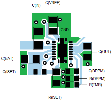 Figure 11. Recommended Layout
11.3 Thermal Considerations
The bq2407x is packaged in a thermally enhanced MLP package. The package includes a QFN thermal pad to provide an effective thermal contact between the device and the printed-circuit board (PCB). Full PCB design guidelines for this package are provided in the application note entitled QFN/SON PCB Attachment (SLUA271). The power pad should be tied to the VSS plane. The most common measure of package thermal performance is thermal impedance (θJA) measured (or modeled) from the chip junction to the air surrounding the package surface (ambient).
The mathematical expression for θJA is:

where
- TJ = chip junction temperature
- TA = ambient temperature
- P = device power dissipation
Factors that can greatly influence the measurement and calculation of θJA include:
- whether or not the device is board mounted
- trace size, composition, thickness, and geometry
- orientation of the device (horizontal or vertical)
- volume of the ambient air surrounding the device under test and airflow
- whether other surfaces are in close proximity to the device being tested
The device power dissipation, P, is a function of the charge rate and the voltage drop across the internal power FET. It can be calculated from Equation 10:

Due to the charge profile of Li-xx batteries, the maximum power dissipation is typically seen at the beginning of the charge cycle when the battery voltage is at its lowest. See Figure 2. Typically the voltage of the Li-ion battery quickly (< 2 V minutes) ramps to approximately 3.5 V, when entering fast charge (1-C charge rate and battery above 3 V). Therefore, it is customary to perform the steady-state thermal design using 3.5 V as the minimum battery voltage because the system board and charging device does not have time to reach a maximum temperature due to the thermal mass of the assembly during the early stages of fast charge. This theory is easily verified by performing a charge cycle on a discharged battery while monitoring the battery voltage and chargers power pad temperature.