SLUS977B September 2009 – August 2015
PRODUCTION DATA.
- 1 Features
- 2 Applications
- 3 Description
- 4 Revision History
- 5 Device Comparison Table
- 6 Pin Configuration and Functions
- 7 Specifications
- 8 Detailed Description
- 9 Application and Implementation
- 10Power Supply Recommendations
- 11Layout
- 12Device and Documentation Support
- 13Mechanical, Packaging, and Orderable Information
Package Options
Mechanical Data (Package|Pins)
- DSG|8
Thermal pad, mechanical data (Package|Pins)
- DSG|8
Orderable Information
8 Detailed Description
8.1 Overview
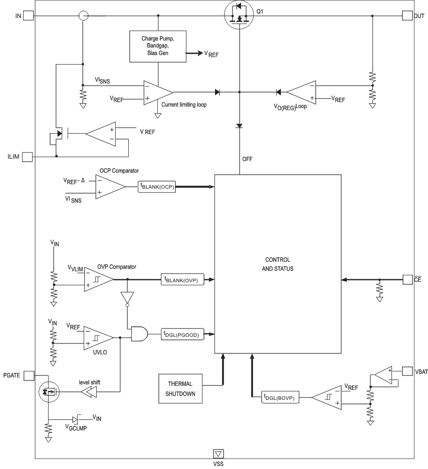
The bq24308 device is a highly integrated circuit designed to provide protection to Li-ion batteries from failures of the charging circuit. The device continuously monitors the input voltage, the input current, and the battery voltage. In case of an input overvoltage condition, the device immediately removes power from the charging circuit by turning off an internal switch. In the case of an overcurrent condition, it limits the current to a safe value for a blanking duration before turning the switch off. Additionally, the device also monitors its own die temperature and switches off if it becomes too hot.
The input and overcurrent threshold is user-programmable. The device can be controlled by a processor using the CE pin.
8.2 Functional Block Diagram

8.3 Feature Description
8.3.1 Input Overvoltage Protection
The bq24308 device integrates an input overvoltage protection feature to protect downstream devices from faulty input sources. If the input voltage rises above VOVP, the internal FET Q1 is turned off, removing power from the circuit. As shown in Figure 16 to Figure 17, the response is very rapid, with the FET turning off in less than a microsecond. When the input voltage returns below VOVP – Vhys(OVP) (but is still above UVLO), the FET Q1 is turned on again after a deglitch time of tON(OVP) to ensure that the input supply has stabilized. Figure 18 shows the recovery from input OVP.
8.3.2 Input Overcurrent Protection
The device can supply load current up to IOCP continuously. If the load current tries to exceed this threshold, the current limits IOCP for a maximum duration of tBLANK(OCP). If the load current returns to less than IOCP before tBLANK(OCP) times out, the device continues to operate (see Figure 19). However, if the overcurrent situation persists for tBLANK(OCP), the FET Q1 is turned off for a duration of tREC(OCP). The FET is then turned on again and the current is monitored all over again (see Figure 20 and Figure 21).
To prevent the input voltage from spiking up due to the inductance of the input cable, Q1 is turned off slowly in an overcurrent fault condition, resulting in a "soft-stop", as shown in Figure 22. The overcurrent threshold is programmed to a level greater than IOCP by connecting a resistor RILIM from the ILIM pin to VSS. The programmed overcurrent threshold is given by the following equation:
8.3.3 Battery Overvoltage Protection
The battery overvoltage threshold BVOVP is internally set to 4.35 V. If the battery voltage exceeds the BVOVP threshold for longer than tDGL(BOVP), the FET Q1 is turned off (see Figure 23). This switch-off is also a soft-stop. The FET Q1 is turned ON (soft-start) once the battery voltage drops to BVOVP – VHYS-BOVP.
8.3.4 Thermal Protection
If the junction temperature of the device exceeds TJ(OFF), FET Q1 is turned off. The FET is turned back on when the junction temperature falls below TJ(OFF) – TJ(OFF-HYS).
8.3.5 Enable Function
The device has an enable pin, which can be used to enable or disable the device. When the CE pin is driven high, the internal FET is turned off. When the CE pin is low, the FET is turned on if other conditions are safe. The CE pin has an internal pulldown resistor of 200 kΩ (typical) and can be left floating.
8.3.6 PGATE Output
The bq24308 contains an external PFET driver (PGATE) for reverse polarity protection. When used with an external P-Channel MOSFET, in addition to OVP, OCP, and Battery-OVP, the device offers protection against input reverse polarity up to –30 V. When an input source with correct polarity is connected, the device first turns on due to current flow through the body-diode of the external FET. The PGATE pin then goes low, turning ON the external FET. For input voltages larger than VGCLMP, the voltage on the PGATE pin is driven to VIN – VGCLMP. This ensures that the gate to source voltage seen by the external FET does not exceed –VGCLMP.
8.4 Device Functional Modes
8.4.1 OPERATION Mode
The bq24308 device continuously monitors the input voltage, the input current, and the battery voltage. As long as the input voltage is less than VOVP, the output voltage tracks the input voltage (less the drop caused by RDSON of Q1). During fault conditions, the internal FET is turned off and the output is isolated from the input source.
8.4.2 POWER-DOWN Mode
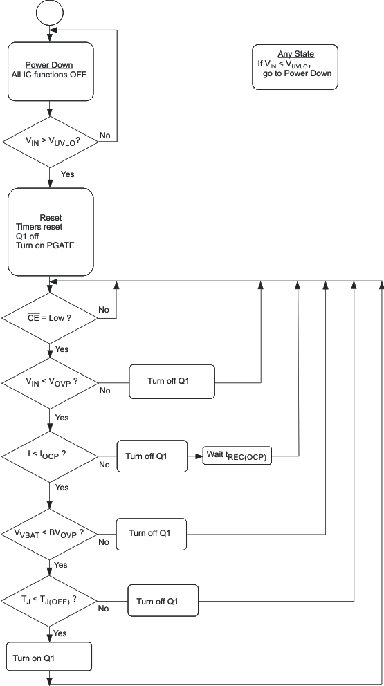
The device remains in POWER-DOWN mode when the input voltage at the IN pin is below the undervoltage lock-out threshold, VUVLO. The FET Q1 (see Functional Block Diagram) connected between IN and OUT pins is off. See Figure 10.
8.4.3 POWER-ON RESET Mode
The device resets all internal timers when the input voltage at the IN pin exceeds the UVLO threshold. The gate driver for the external P-FET is enabled. The device then waits for duration tDGL(PGOOD) for the input voltage to stabilize. If, after tDGL(PGOOD), the input voltage and battery voltage are safe, FET Q1 is turned ON. The device has a soft-start feature to control the inrush current. This soft-start minimizes voltage ringing at the input (the ringing occurs because the parasitic inductance of the adapter cable and the input bypass capacitor form a resonant circuit). Figure 14 shows the power-up behavior of the device. Because of the deglitch time at power-on, if the input voltage rises rapidly to beyond the OVP threshold, the device will not switch on at all, as shown in Figure 15.
 Figure 10. State Diagram