SLUSAH0G october   2011  – august 2023 BQ25504

PRODUCTION DATA  

  1.   1
  2. Features
  3. Applications
  4. Description
  5. Revision History
  6. Description (continued)
  7. Pin Configuration and Functions
  8. Specifications
    1. 7.1 Absolute Maximum Ratings
    2. 7.2 ESD Ratings
    3. 7.3 Recommended Operating Conditions
    4. 7.4 Thermal Information
    5. 7.5 Electrical Characteristics
    6. 7.6 Typical Characteristics
  9. Detailed Description
    1. 8.1 Overview
    2. 8.2 Functional Block Diagram
    3. 8.3 Feature Description
      1. 8.3.1 Maximum Power Point Tracking
      2. 8.3.2 Battery Undervoltage Protection
      3. 8.3.3 Battery Overvoltage Protection
      4. 8.3.4 Battery Voltage in Operating Range (VBAT_OK Output)
      5. 8.3.5 Nano-Power Management and Efficiency
    4. 8.4 Device Functional Modes
      1. 8.4.1 Cold-Start Operation (VSTOR < VSTOR_CHGEN, VIN_DC > VIN(CS) and PIN > PIN(CS))
      2. 8.4.2 Main Boost Charger Enabled (VSTOR > VSTOR_CHGEN, VIN_DC > VIN(DC) and EN = LOW )
      3. 8.4.3 Thermal Shutdown
  10. Application and Implementation
    1. 9.1 Application Information
      1. 9.1.1 Storage Element Selection
      2. 9.1.2 Inductor Selection
      3. 9.1.3 Capacitor Selection
        1. 9.1.3.1 VREF_SAMP Capacitance
        2. 9.1.3.2 VIN_DC Capacitance
        3. 9.1.3.3 VSTOR Capacitance
        4. 9.1.3.4 Additional Capacitance on VSTOR or VBAT
    2. 9.2 Typical Applications
      1. 9.2.1 Solar Application Circuit
        1. 9.2.1.1 Design Requirements
        2. 9.2.1.2 Detailed Design Procedure
        3. 9.2.1.3 Application Curves
      2. 9.2.2 TEG Application Circuit
        1. 9.2.2.1 Design Requirements
        2. 9.2.2.2 Detailed Design Procedure
        3. 9.2.2.3 Application Curves
      3. 9.2.3 MPPT Disabled, Low Impedance Source Application Circuit
        1. 9.2.3.1 Design Requirements
        2. 9.2.3.2 Detailed Design Procedure
        3. 9.2.3.3 Application Curves
  11. 10Power Supply Recommendations
  12. 11Layout
    1. 11.1 Layout Guidelines
    2. 11.2 Layout Example
    3. 11.3 Thermal Considerations
  13. 12Device and Documentation Support
    1. 12.1 Device Support
      1. 12.1.1 Third-Party Products Disclaimer
      2. 12.1.2 Zip Files
    2. 12.2 Documentation Support
      1. 12.2.1 Related Documentation
    3. 12.3 Receiving Notification of Documentation Updates
    4. 12.4 Support Resources
    5. 12.5 Trademarks
    6. 12.6 Electrostatic Discharge Caution
    7. 12.7 Glossary
  14. 13Mechanical, Packaging, and Orderable Information

Package Options

Mechanical Data (Package|Pins)
Thermal pad, mechanical data (Package|Pins)
Orderable Information

Maximum Power Point Tracking

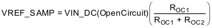
Maximum power point tracking (MPPT) is implemented in order to maximize the power extracted from an energy harvester source. The boost converter indirectly modulates the input impedance of the main boost charger by regulating the charger's input voltage, as sensed by the VIN_DC pin, to the sampled reference voltage stored on the VREF_SAMP pin. The MPPT circuit obtains a new reference voltage every 16 s (typical) by periodically disabling the charger for 256 ms (typical) and sampling a fraction of the harvester's open-circuit voltage (VOC). For solar harvesters, the maximum power point is typically 70%-80% of VOC and for thermoelectric harvesters, the MPPT is typically 50%. The exact ratio for MPPT can be optimized to meet the needs of the input source being used by connecting external resistors ROC1 and ROC2 between VIN_DC and GND with mid-point at VOC_SAMP.

Equation 1. GUID-EF51510E-8575-44E5-BEB7-BB493623E78B-low.gif

Spreadsheet SLUC484 provides help on sizing and selecting the resistors.

The internal MPPT circuitry and the periodic sampling of VIN_DC can be disabled by tying the VOC_SAMP pin to VSTOR. An external reference voltage can be fed to the VREF_SAMP pin. The boost converter will then regulate VIN_DC to the externally provided reference. If input regulation is not desired (i.e. the input source is a low-impedance output battery or power supply instead of a high impedance output energy harvester), VREF_SAMP can be tied to GND.