SLUSAH0G october   2011  – august 2023 BQ25504

PRODUCTION DATA  

  1.   1
  2. Features
  3. Applications
  4. Description
  5. Revision History
  6. Description (continued)
  7. Pin Configuration and Functions
  8. Specifications
    1. 7.1 Absolute Maximum Ratings
    2. 7.2 ESD Ratings
    3. 7.3 Recommended Operating Conditions
    4. 7.4 Thermal Information
    5. 7.5 Electrical Characteristics
    6. 7.6 Typical Characteristics
  9. Detailed Description
    1. 8.1 Overview
    2. 8.2 Functional Block Diagram
    3. 8.3 Feature Description
      1. 8.3.1 Maximum Power Point Tracking
      2. 8.3.2 Battery Undervoltage Protection
      3. 8.3.3 Battery Overvoltage Protection
      4. 8.3.4 Battery Voltage in Operating Range (VBAT_OK Output)
      5. 8.3.5 Nano-Power Management and Efficiency
    4. 8.4 Device Functional Modes
      1. 8.4.1 Cold-Start Operation (VSTOR < VSTOR_CHGEN, VIN_DC > VIN(CS) and PIN > PIN(CS))
      2. 8.4.2 Main Boost Charger Enabled (VSTOR > VSTOR_CHGEN, VIN_DC > VIN(DC) and EN = LOW )
      3. 8.4.3 Thermal Shutdown
  10. Application and Implementation
    1. 9.1 Application Information
      1. 9.1.1 Storage Element Selection
      2. 9.1.2 Inductor Selection
      3. 9.1.3 Capacitor Selection
        1. 9.1.3.1 VREF_SAMP Capacitance
        2. 9.1.3.2 VIN_DC Capacitance
        3. 9.1.3.3 VSTOR Capacitance
        4. 9.1.3.4 Additional Capacitance on VSTOR or VBAT
    2. 9.2 Typical Applications
      1. 9.2.1 Solar Application Circuit
        1. 9.2.1.1 Design Requirements
        2. 9.2.1.2 Detailed Design Procedure
        3. 9.2.1.3 Application Curves
      2. 9.2.2 TEG Application Circuit
        1. 9.2.2.1 Design Requirements
        2. 9.2.2.2 Detailed Design Procedure
        3. 9.2.2.3 Application Curves
      3. 9.2.3 MPPT Disabled, Low Impedance Source Application Circuit
        1. 9.2.3.1 Design Requirements
        2. 9.2.3.2 Detailed Design Procedure
        3. 9.2.3.3 Application Curves
  11. 10Power Supply Recommendations
  12. 11Layout
    1. 11.1 Layout Guidelines
    2. 11.2 Layout Example
    3. 11.3 Thermal Considerations
  13. 12Device and Documentation Support
    1. 12.1 Device Support
      1. 12.1.1 Third-Party Products Disclaimer
      2. 12.1.2 Zip Files
    2. 12.2 Documentation Support
      1. 12.2.1 Related Documentation
    3. 12.3 Receiving Notification of Documentation Updates
    4. 12.4 Support Resources
    5. 12.5 Trademarks
    6. 12.6 Electrostatic Discharge Caution
    7. 12.7 Glossary
  14. 13Mechanical, Packaging, and Orderable Information

Package Options

Mechanical Data (Package|Pins)
Thermal pad, mechanical data (Package|Pins)
Orderable Information

Battery Undervoltage Protection

To prevent rechargeable batteries from being deeply discharged and damaged, and to prevent completely depleting charge from a capacitive storage element, the undervoltage (VBAT_UV) threshold must be set using external resistors. The VBAT_UV threshold voltage when the battery voltage is decreasing is given by Equation 2:

Equation 2. GUID-F1D98591-3B7F-4330-BC93-50B5C5B36EB1-low.gif

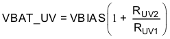
The sum of the resistors is recommended to be no higher than 10 MΩ that is, RUV1 + RUV2 = 10 MΩ. Spreadsheet SLURAQ1 provides help on sizing and selecting the resistors.

The undervoltage threshold when the battery voltage is increasing is VBAT_UV plus an internal hysteresis voltage denoted by VBAT_UV_HYST. For the VBAT_UV feature to function properly, the load must be connected to the VSTOR pin while the storage element should be connected to the VBAT pin. Once the VSTOR pin voltage goes above VBAT_UV plus VBAT_UV_HYST threshold, the VSTOR pin and the VBAT pins are effectively shorted through an internal PMOS FET. The switch remains closed until the VSTOR pin voltage falls below the VBAT_UV threshold. The VBAT_UV threshold should be considered a fail safe to the system. The system load should be removed or reduced based on the VBAT_OK threshold which should be set above the VBAT_UV threshold.