SLUSEN5 august 2023 BQ25756
PRODUCTION DATA
- 1
- 1 Features
- 2 Applications
- 3 Description
- 4 Revision History
- 5 Description (continued)
- 6 Pin Configuration and Functions
- 7 Specifications
-
8 Detailed Description
- 8.1 Overview
- 8.2 Functional Block Diagram
- 8.3
Feature Description
- 8.3.1 Device Power-On-Reset
- 8.3.2 Device Power-Up From Battery Without Input Source
- 8.3.3 Device Power Up from Input Source
- 8.3.4 Battery Charging Management
- 8.3.5 Power Management
- 8.3.6 Reverse Mode Power Direction
- 8.3.7 Integrated 16-Bit ADC for Monitoring
- 8.3.8 Status Outputs (PG, STAT1, STAT2, and INT)
- 8.3.9
Protections
- 8.3.9.1
Voltage and Current Monitoring
- 8.3.9.1.1 VAC Over-voltage Protection (VAC_OVP)
- 8.3.9.1.2 VAC Under-voltage Protection (VAC_UVP)
- 8.3.9.1.3 Battery Over-voltage Protection (BAT_OVP)
- 8.3.9.1.4 Battery Over-current Protection (BAT_OCP)
- 8.3.9.1.5 Reverse Mode Over-voltage Protection (REV_OVP)
- 8.3.9.1.6 Reverse Mode Under-voltage Protection (REV_UVP)
- 8.3.9.1.7 DRV_SUP Under-voltage and Over-voltage Protection (DRV_OKZ)
- 8.3.9.1.8 REGN Under-voltage Protection (REGN_OKZ)
- 8.3.9.2 Thermal Shutdown (TSHUT)
- 8.3.9.1
Voltage and Current Monitoring
- 8.3.10 Serial Interface
- 8.4 Device Functional Modes
- 8.5 BQ25756 Registers
-
9 Application and Implementation
- 9.1 Application Information
- 9.2
Typical Applications
- 9.2.1
Typical Application
- 9.2.1.1 Design Requirements
- 9.2.1.2
Detailed Design Procedure
- 9.2.1.2.1 ACUV / ACOV Input Voltage Operating Window Programming
- 9.2.1.2.2 Charge Voltage Selection
- 9.2.1.2.3 Switching Frequency Selection
- 9.2.1.2.4 Inductor Selection
- 9.2.1.2.5 Input (VAC) Capacitor
- 9.2.1.2.6 Output (VBAT) Capacitor
- 9.2.1.2.7 Sense Resistor (RAC_SNS and RBAT_SNS) and Current Programming
- 9.2.1.2.8 Power MOSFETs Selection
- 9.2.1.2.9 Converter Fast Transient Response
- 9.2.1.3 Application Curves
- 9.2.2 Typical Application (USB-PD EPR Configuration)
- 9.2.1
Typical Application
- 10Power Supply Recommendations
- 11Layout
- 12Device and Documentation Support
- 13Mechanical, Packaging, and Orderable Information
Package Options
Mechanical Data (Package|Pins)
- RRV|36
Thermal pad, mechanical data (Package|Pins)
- RRV|36
Orderable Information
8.3.4.7.1 JEITA Guideline Compliance in Charge Mode
To improve the safety of charging Li-ion batteries, JEITA guideline was released on April 20, 2007. The guideline emphasized the importance of avoiding a high charge current and high charge voltage at certain low and high temperature ranges.
To initiate a charge cycle, the voltage on TS pin must be within the VT1 to VT5 thresholds. If TS voltage exceeds the T1 to T5 range, the controller suspends charging and waits until the battery temperature is within the T1 to T5 range.
At cool temperature, T1 to T2, JEITA recommends the charge current to be reduced to half of the charge current or lower. The device allows charge current in the cool temperature region to be progrramed to 20%, 40% or 100% of the charge current at T2 to T3 or charge suspend, which is controlled by the register bits JEITA_ISETC. If charge current is reduced in the cool temperature region, the safety timer counts at half clock rate when EN_TMR2X = 1.
At warm temperature, T3 to T5, JEITA recommends charge voltage less than 4.1 V / cell. The device provides the programmability of the charge voltage at T3-T5, to be with a voltage offset less than charge voltage at T2 to T3 or charge suspend, which is controlled by the register bits JEITA_VSET.
The charger also provides flexible voltage/current settings beyond the JEITA requirements. The charge current setting at warm temperature T3 to T5 can be configured to be 40%, or 100% of the programmed charge current or charge suspend, which is programmed by the register bit JEITA_ISETH. If charge current is reduced in the JEITA warm region, the safety timer counts at half clock rate when EN_TMR2X = 1.
The default charging profile for JEITA is shown in the figure below, in which the blue line is the default setting and the red dash line is the programmable options.
 Figure 8-4 TS Charging Values
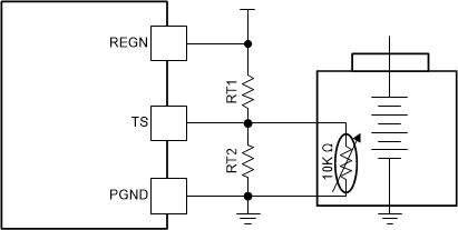
Assuming a 103AT NTC thermistor on the battery pack as shown above, the value of RT1 and RT2 can be determined by:
Select 0°C to 60°C range for Li-ion or Li-polymer battery:
RTHT1 = 27.28 kΩ
RTHT5 = 3.02 kΩ
RT1 = 5.24 kΩ
RT2 = 30.31 kΩ
The device also offers programmability for all the thresholds via the TS Charging Threshold Control register (REG0x1B). This flexibility can help to change the charger's operating window in software.
The JEITA profile can be disabled by clearing the EN_JEITA register bit. In this case, the device still limits the charging window from T1 to T5, but no special charge profile is employed within the Cool (T1 to T2) or Warm (T3 to T5) regions.
The NTC monitoring window can be disabled by clearing the EN_TS register bit. In this case, the TS pin voltage is ignored, and the device always reports normal TS status. If EN_TS is set to 0, TS pin can be floated or connected to PGND.