SLUS900E December 2008 – August 2015
PRODUCTION DATA.
- 1 Features
- 2 Applications
- 3 Description
- 4 Revision History
- 5 Pin Configuration and Functions
- 6 Specifications
-
7 Detailed Description
- 7.1 Overview
- 7.2 Functional Block Diagram
- 7.3 Feature Description
- 7.4 Device Functional Modes
- 7.5 Programming
- 7.6
Register Maps
- 7.6.1 I2C Read After Backup Mode
- 7.6.2
Normal Register Descriptions
- 7.6.2.1 SECONDS Register (address = 0x00) [reset = 0XXXXXXb]
- 7.6.2.2 MINUTES Register (address = 0x01) [reset = 1XXXXXXb]
- 7.6.2.3 CENT_HOURS Register (address = 0x02) [reset = XXXXXXXXb]
- 7.6.2.4 DAY Register (address = 0x03) [reset = 00000XXXb]
- 7.6.2.5 DATE Register (address = 0x04) [reset = 00XXXXXXb]
- 7.6.2.6 MONTH Register (address = 0x05) [reset = 000XXXXXb]
- 7.6.2.7 YEARS Register (address = 0x06) [reset = XXXXXXXXb]
- 7.6.2.8 CAL_CFG1 Register (address = 0x07) [reset = 10000000b]
- 7.6.2.9 TCH2 Register (address = 0x08) [reset = 10010000b]
- 7.6.2.10 CFG2 Register (address = 0x09) [reset = 10101010b]
- 7.6.3 Special Function Registers
- 8 Application and Implementation
- 9 Power Supply Recommendations
- 10Layout
- 11Device and Documentation Support
- 12Mechanical, Packaging, and Orderable Information
Package Options
Mechanical Data (Package|Pins)
- D|8
Thermal pad, mechanical data (Package|Pins)
Orderable Information
6 Specifications
6.1 Absolute Maximum Ratings(1)
over operating free-air temperature range (unless otherwise noted)| MIN | MAX | UNIT | |||
|---|---|---|---|---|---|
| Input voltage, VIN | VCC to GND | –0.3 | 4 | V | |
| All other pins to GND | –0.3 | VCC + 0.3 | V | ||
| Operating junction temperature, TJ | –40 | 150 | °C | ||
| Storage temperature, Tstg | –60 | 150 | °C | ||
(1) Stresses beyond those listed under absolute maximum ratings may cause permanent damage to the device. These are stress ratings only, and functional operation of the device at these or any other conditions beyond those indicated under recommended operating conditions is not implied. Exposure to absolute-maximum-rated conditions for extended periods may affect device reliability.
6.2 ESD Ratings
| VALUE | UNIT | |||
|---|---|---|---|---|
| V(ESD) | Electrostatic discharge | Human body model (HBM), per ANSI/ESDA/JEDEC JS-001, all pins(1) | 2000 | V |
| Charged device model (CDM), per JEDEC specification JESD22-C101, all pins(2) | 500 | |||
(1) JEDEC document JEP155 states that 500-V HBM allows safe manufacturing with a standard ESD control process.
(2) JEDEC document JEP157 states that 250-V CDM allows safe manufacturing with a standard ESD control process.
6.3 Recommended Operating Conditions
| MIN | NOM | MAX | UNIT | ||
|---|---|---|---|---|---|
| VCC | Supply voltage, VCC to GND | 3 | 3.6 | V | |
| TA | Operating free-air temperature | –40 | 85 | °C | |
| fo | Crystal resonant frequency | 32.768 | kHz | ||
| RS | Crystal series resistance | 70 | kΩ | ||
| CL | Crystal load capacitance | 10.8 | 12 | 13.2 | pF |
6.4 Thermal Information
over operating free-air temperature range (unless otherwise noted)| THERMAL METRIC(1) | bq32000 | UNIT | |||
|---|---|---|---|---|---|
| D (SOIC) | |||||
| 8 PINS | |||||
| RθJA | Junction-to-ambient thermal resistance | 114.8 | °C/W | ||
| RθJC(top) | Junction-to-case (top) thermal resistance | 59.1 | °C/W | ||
| RθJB | Junction-to-board thermal resistance | 55.5 | °C/W | ||
| ψJT | Junction-to-top characterization parameter | 11.9 | °C/W | ||
| ψJT | Junction-to-board characterization parameter | 55 | °C/W | ||
(1) For more information about traditional and new thermal metrics, see the Semiconductor and IC Package Thermal Metrics application report, SPRA953.
6.5 Electrical Characteristics
over operating free-air temperature range (unless otherwise noted)| PARAMETER | TEST CONDITIONS | MIN | TYP | MAX | UNIT | |
|---|---|---|---|---|---|---|
| POWER SUPPLY | ||||||
| ICC | VCC supply current | 100 | μA | |||
| VBACK | Backup supply voltage | Operating | 1.4 | VCC | V | |
| Switchover | 2.0 | VCC | ||||
| IBACK | Backup supply current | VCC needs a pulse (1), VBACK = 3 V, Oscillator on, TA = 25°C | 1.2 | 1.5 | μA | |
| LOGIC LEVEL INPUTS | ||||||
| VIL | Input low voltage | 0.3 VCC | V | |||
| VIH | Input high voltage | 0.7 VCC | V | |||
| IIN | Input current | 0 V ≤ VIN ≤ VCC | -1 | 1 | μA | |
| LOGIC LEVEL OUTPUTS | ||||||
| VOL | Output low voltage | IOL = 3 mA | 0.4 | V | ||
| IL | Leakage current | -1 | 1 | μA | ||
| REAL-TIME CLOCK CHARACTERISTICS | ||||||
| Pre-calibration accuracy | VCC = 3.3 V, VBACK = 3 V, Oscillator on, TA = 25°C | ±35(2) | ppm | |||
(1) The currents measured after issuing a pulse on VCC. The pulse amplitude 0-VCC; pulse width min 1 ms.
(2) Typical accuracy is measured using reference board design and KDS DMX-26S surface-mount 32.768-kHz crystal. Variation in board design and crystal section results in different typical accuracy.
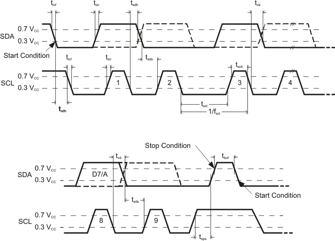
6.6 I2C Timing Requirements
| STANDARD MODE | FAST MODE | UNIT | ||||
|---|---|---|---|---|---|---|
| MIN | MAX | MIN | MAX | |||
| fscl | I2C clock frequency | 0 | 100 | 0 | 400 | kHz |
| tsch | I2C clock high time | 4 | 0.6 | μs | ||
| tscl | I2C clock low time | 4.7 | 1.3 | μs | ||
| tsp | I2C spike time | 0 | 50 | 0 | 50 | ns |
| tsds | I2C serial data setup time | 250 | 100 | ns | ||
| tsdh | I2C serial data hold time | 0 | 0 | ns | ||
| ticr | I2C input rise time | 1000 | 20 + 0.1Cb(1) | 300 | ns | |
| ticf | I2C input fall time | 300 | 20 + 0.1Cb(1) | 300 | ns | |
| tocf | I2C output fall time | 300 | 20 + 0.1Cb(1) | 300 | μs | |
| tbuf | I2C bus free time | 4.7 | 1.3 | μs | ||
| tsts | I2C Start setup time | 4.7 | 0.6 | μs | ||
| tsth | I2C Start hold time | 4 | 0.6 | μs | ||
| tsps | I2C Stop setup time | 4 | 0.6 | μs | ||
| tvd(data) | Valid data time (SCL low to SDA valid) | 1 | 1 | μs | ||
| tvd(ack) | Valid data time of ACK (ACK signal from SCL low to SDA low) |
1 | 1 | μs | ||
(1) Cb = total capacitance of one bus line in pF
 Figure 1. I2C Timing Diagram
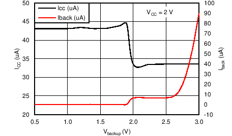
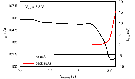
6.7 Typical Characteristics

