SLUSCS4C June 2017 – April 2021 BQ40Z50-R2
PRODUCTION DATA
- 1 Features
- 2 Applications
- 3 Description
- 4 Revision History
- 5 Description (continued)
- 6 Pin Configuration and Functions
-
7 Specifications
- 7.1 Absolute Maximum Ratings
- 7.2 ESD Ratings
- 7.3 Recommended Operating Conditions
- 7.4 Thermal Information
- 7.5 Supply Current
- 7.6 Power Supply Control
- 7.7 AFE Power-On Reset
- 7.8 AFE Watchdog Reset and Wake Timer
- 7.9 Current Wake Comparator
- 7.10 VC1, VC2, VC3, VC4, BAT, PACK
- 7.11 SMBD, SMBC
- 7.12 PRES, BTP_INT, DISP
- 7.13 LEDCNTLA, LEDCNTLB, LEDCNTLC
- 7.14 Coulomb Counter
- 7.15 CC Digital Filter
- 7.16 ADC
- 7.17 ADC Digital Filter
- 7.18 CHG, DSG FET Drive
- 7.19 PCHG FET Drive
- 7.20 FUSE Drive
- 7.21 Internal Temperature Sensor
- 7.22 TS1, TS2, TS3, TS4
- 7.23 PTC, PTCEN
- 7.24 Internal 1.8-V LDO
- 7.25 High-Frequency Oscillator
- 7.26 Low-Frequency Oscillator
- 7.27 Voltage Reference 1
- 7.28 Voltage Reference 2
- 7.29 Instruction Flash
- 7.30 Data Flash
- 7.31 OLD, SCC, SCD1, SCD2 Current Protection Thresholds
- 7.32 Timing Requirements: OLD, SCC, SCD1, SCD2 Current Protection Timing
- 7.33 Timing Requirements: SMBus
- 7.34 Timing Requirements: SMBus XL
- 7.35 Typical Characteristics
-
8 Detailed Description
- 8.1 Overview
- 8.2 Functional Block Diagram
- 8.3
Feature Description
- 8.3.1 Primary (1st Level) Safety Features
- 8.3.2 Secondary (2nd Level) Safety Features
- 8.3.3 Charge Control Features
- 8.3.4 Gas Gauging
- 8.3.5 Configuration
- 8.3.6 Battery Parameter Measurements
- 8.3.7 Battery Trip Point (BTP)
- 8.3.8 Lifetime Data Logging Features
- 8.3.9 Authentication
- 8.3.10 LED Display
- 8.3.11 IATA Support
- 8.3.12 Voltage
- 8.3.13 Current
- 8.3.14 Temperature
- 8.3.15 Communications
- 8.4 Device Functional Modes
- 9 Application and Implementation
- 10Power Supply Recommendations
- 11Layout
- 12Device and Documentation Support
- 13Mechanical, Packaging, and Orderable Information
Package Options
Mechanical Data (Package|Pins)
- RSM|32
Thermal pad, mechanical data (Package|Pins)
- RSM|32
Orderable Information
9.2.2.2.5 FUSE Circuitry
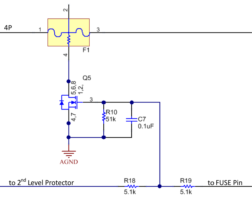
The FUSE pin of the BQ40Z50-R2 device is designed to ignite the chemical fuse if one of the various safety criteria is violated. The FUSE pin also monitors the state of the secondary-voltage protection IC. Q5 ignites the chemical fuse when its gate is high. The 7-V output of the bq294700 is divided by R18 and R19, which provides adequate gate drive for Q5 while guarding against excessive back current into the bq294700 if the FUSE signal is high.
Using C7 is generally a good practice, especially for RFI immunity. C7 may be removed, if desired, because the chemical fuse is a comparatively slow device and is not affected by any sub-microsecond glitches that come from the FUSE output during the cell connection process.
If the AFEFUSE output is not used, it should be connected to VSS.
 Figure 9-11 FUSE Circuit
When the BQ40Z50-R2 device is commanded to ignite the chemical fuse, the FUSE pin activates to give a typical 8-V output. The new design makes it possible to use a higher Vgs FET for Q5. This improves the robustness of the system, as well as widens the choices for Q5.