SLUSBB1B December 2012 – June 2016
- 1 Features
- 2 Applications
- 3 Description
- 4 Revision History
- 5 Pin Configuration and Functions
- 6 Specifications
-
7 Detailed Description
- 7.1 Overview
- 7.2 Functional Block Diagram
- 7.3
Feature Description
- 7.3.1 Dynamic Power Limiting™
- 7.3.2 Option Select Pin
- 7.3.3 LED Indication Modes
- 7.3.4 Parasitic Metal Object Detect (PMOD) and Foreign Object Detection (FOD)
- 7.3.5 Shut Down via External Thermal Sensor or Trigger
- 7.3.6 Fault Handling and Indication
- 7.3.7 Power Transfer Start Signal
- 7.3.8 Power-On Reset
- 7.3.9 External Reset, RESET Pin
- 7.3.10 Trickle Charge and CS100
- 7.3.11 Current Monitoring Requirements
- 7.3.12 Overcurrent Protection
- 7.3.13 MSP430G2001 Low Power Supervisor
- 7.3.14 All Unused Pins
- 8 Application and Implementation
- 9 Layout
- 10Device and Documentation Support
- 11Mechanical, Packaging, and Orderable Information
Package Options
Mechanical Data (Package|Pins)
- RGZ|48
Thermal pad, mechanical data (Package|Pins)
- RGZ|48
Orderable Information
1 Features
- Intelligent Control of Wireless Power Transfer
- 5-V Operation Conforms to Wireless Power Consortium (WPC) Type A5 and Type A11 Transmitter Specifications
- WPC1.1 Compliant, Including Foreign Object Detection (FOD)
- Enhanced Parasitic Metal Detection (PMOD) Assures Safety
- Dynamic Power Limiting™ for USB and Limited Source Operation
- Digital Demodulation Reduces Components
- LED Indication of Charging State and Fault Status
2 Applications
- WPC 1.1 Compliant Wireless Chargers For:
- Qi-Certified Smart Phones and other Handhelds
- Hermetically Sealed Devices and Tools
- Cars and Other Vehicles
- Tabletop Charge Surfaces
- See www.ti.com/wirelesspower for More Information on TI's Wireless Charging Solutions
3 Description
The bq500211A is a second generation digital wireless power controller that integrates all functions required to control wireless power transfer to a single WPC compliant receiver. It is WPC1.1 compliant and designed for 5-V systems as either a WPC type A5 transmitter with a magnetic positioning guide or as a WPC type A11 transmitter without the magnetic guide. The bq500211A pings the surrounding environment for WPC compliant devices to be powered, safely engages the device, receives packet communication from the powered device and manages the power transfer. To maximize flexibility in wireless power applications, Dynamic Power Limiting™ (DPL) is featured on the bq500211A. DPL enhances user experience by seamlessly optimizing the usage of power available from limited input supplies. The bq500211A supports both Foreign Object Detection (FOD) and Parasitic Metal Object Detection (PMOD) by continuously monitoring the efficiency of the established power transfer, protecting from power lost due to metal objects misplaced in the wireless power transfer bath. Should any abnormal condition develop during power transfer, the bq500211A handles it and provides indicator outputs. Comprehensive status and fault monitoring features enable a robust system design.
The bq500211A is available in a 48-pin, 7 mm x 7 mm QFN package and operates over a temperature range from –40°C to 110°C.
Device Information(1)
| PART NUMBER | PACKAGE | BODY SIZE (NOM) |
|---|---|---|
| bq500211A | VQFN (48) | 7.00 mm × 7.00 mm |
- For all available packages, see the orderable addendum at the end of the data sheet.
Functional Diagram

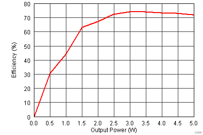
Efficiency vs System Output Power
