SLUSBB1B December 2012 – June 2016
- 1 Features
- 2 Applications
- 3 Description
- 4 Revision History
- 5 Pin Configuration and Functions
- 6 Specifications
-
7 Detailed Description
- 7.1 Overview
- 7.2 Functional Block Diagram
- 7.3
Feature Description
- 7.3.1 Dynamic Power Limiting™
- 7.3.2 Option Select Pin
- 7.3.3 LED Indication Modes
- 7.3.4 Parasitic Metal Object Detect (PMOD) and Foreign Object Detection (FOD)
- 7.3.5 Shut Down via External Thermal Sensor or Trigger
- 7.3.6 Fault Handling and Indication
- 7.3.7 Power Transfer Start Signal
- 7.3.8 Power-On Reset
- 7.3.9 External Reset, RESET Pin
- 7.3.10 Trickle Charge and CS100
- 7.3.11 Current Monitoring Requirements
- 7.3.12 Overcurrent Protection
- 7.3.13 MSP430G2001 Low Power Supervisor
- 7.3.14 All Unused Pins
- 8 Application and Implementation
- 9 Layout
- 10Device and Documentation Support
- 11Mechanical, Packaging, and Orderable Information
Package Options
Mechanical Data (Package|Pins)
- RGZ|48
Thermal pad, mechanical data (Package|Pins)
- RGZ|48
Orderable Information
7 Detailed Description
7.1 Overview
7.1.1 Fundamentals
The principle of wireless power transfer is simply an open cored transformer consisting of primary and secondary coils and associated electronics. The primary coil and electronics are also referred to as the transmitter, and the secondary side the receiver. The transmitter coil and electronics are typically built into a charger pad. The receiver coil and electronics are typically built into a portable device, such as a cell-phone.
When the receiver coil is positioned on the transmitter coil, magnetic coupling occurs when the transmitter coil is driven. The flux is coupled into the secondary coil which induces a voltage, current flows, it is rectified and power can be transferred quite effectively to a load - wirelessly. Power transfer can be managed via any of various familiar closed-loop control schemes.
7.1.2 Wireless Power Consortium (WPC)
The Wireless Power Consortium (WPC) is an international group of companies from diverse industries. The WPC standard was developed to facilitate cross compatibility of compliant transmitters and receivers. The standard defines the physical parameters and the communication protocol to be used in wireless power. For more information, go to www.wirelesspowerconsortium.com.
7.1.3 Power Transfer
Power transfer depends on coil coupling. Coupling is dependant on the distance between coils, alignment, coil dimensions, coil materials, number of turns, magnetic shielding, impedance matching, frequency and duty cycle.
Most importantly, the receiver and transmitter coils must be aligned for best coupling and efficient power transfer. The closer the space between the coils, the better the coupling, but the practical distance is set to be less than 5 mm (as defined within the WPC Specification) to account for housing and interface surfaces.
Shielding is added as a backing to both the transmitter and receiver coils to direct the magnetic field to the coupled zone. Magnetic fields outside the coupled zone do not transfer power. Thus, shielding also serves to contain the fields to avoid coupling to other adjacent system components.
Regulation can be achieved by controlling any one of the coil coupling parameters. For WPC compatibility, the transmitter coils and capacitance are specified and the resonant frequency point is fixed at 100 kHz. Power transfer is regulated by changing the operating frequency between 112 kHz to 205 kHz. The higher the frequency, the further from resonance and the lower the power. Duty cycle remains constant at 50% throughout the power band and is reduced only once 205 kHz is reached.
The WPC standard describes the dimension and materials of the coils. It also has information on tuning the coils to resonance. The value of the inductor and resonant capacitor are critical to proper operation and system efficiency.
7.1.4 Communication
Communication within the WPC is from the receiver to the transmitter, where the receiver tells the transmitter to send power and how much. In order to regulate, the receiver must communicate with the transmitter whether to increase or decrease frequency. The receiver monitors the rectifier output and using Amplitude Modulation (AM), sends packets of information to the transmitter. A packet is comprised of a preamble, a header, the actual message and a checksum, as defined by the WPC standard.
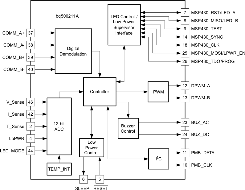
The receiver sends a packet by modulating an impedance network. This AM signal reflects back as a change in the voltage amplitude on the transmitter coil. The signal is demodulated and decoded by the transmitter side electronics and the frequency of its coil drive output is adjusted to close the regulation loop. The bq500211A features internal digital demodulation circuitry.
The modulated impedance network on the receiver can either be resistive or capacitive. Figure 3 shows the resistive modulation approach, where a resistor is periodically added to the load and also shows the resulting change in resonant curve which causes the amplitude change in the transmitter voltage indicated by the two operating points at the same frequency. Figure 4 shows the capacitive modulation approach, where a capacitor is periodically added to the load and also shows the resulting amplitude change in the transmitter voltage.
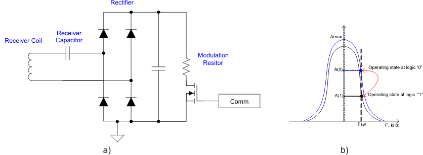 Figure 3. Receiver Resistive Modulation Circuit
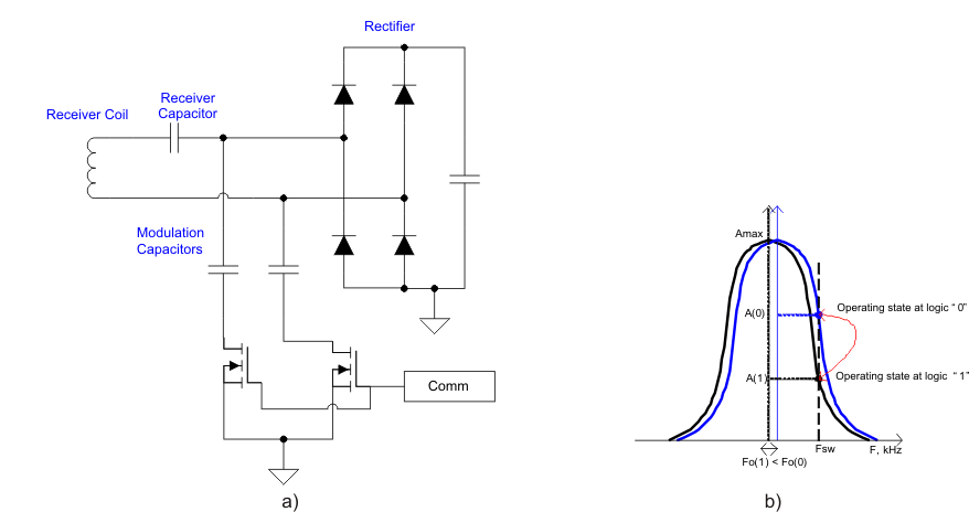 Figure 4. Receiver Capacitive Modulation Circuit
7.2 Functional Block Diagram
7.3 Feature Description
7.3.1 Dynamic Power Limiting™
Dynamic Power Limiting™ (DPL) allows operation from a 5-V supply with limited current capability (such as a USB port). There are two modes of operation selected via an input pin. In the dynamic mode, when the input voltage is observed drooping, the output power is limited to reduce the load and provides margin relative to the supply’s capability. The second mode, or constant current mode, is designed specifically for operation from a 500-mA capable USB port, it restricts the output such that the input current remains below the 500-mA limit.
NOTE
Pin 4 must always be terminated, else erratic behavior may result.
Anytime the DPL control loop is regulating the operating point of the transmitter, the LED will indicate that DPL is active. The LED color and flashing pattern are determined by the LED Table. If the receiver sends a Control Error Packet (CEP) with a negative value, (for example, to reduce power to the load), the WPTX in DPL mode will respond to this CEP via the normal WPC control loop.
NOTE
Depending on LED_MODE selected, the power limit indication may be either solid amber (green + red) or solid red.
7.3.2 Option Select Pin
Two pins (pin 43 and pin 44) on the bq500211A are allocated to program the Loss Threshold and the LED mode of the device. At power up, a bias current is applied to pins LED_MODE and LOSS_THR and the resulting voltage measured in order to identify the value of the attached programming resistor. The values of the operating parameters set by these pins are determined using Table 2. For LED_MODE, the selected bin determines the LED behavior based on Table 1; for the LOSS_THR, the selected bin sets a threshold used for parasitic metal object detection (see Parasitic Metal Detection (PMOD) and Foreign Object Detection (FOD) section). Table 1.
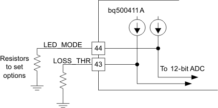 Figure 5. Option Select Pin Programming
7.3.3 LED Indication Modes
The bq500211A can directly drive two LED outputs (pin 7 and pin 8) through a simple current limit resistor (typically 470 Ω), based on the mode selected. The two current limit resistors can be individually adjusted to tune or match the brightness of the two LEDs. Do not exceed the maximum output current rating of the device.
The resistor in Figure 5 connected to pin 44 and GND selects the desired LED indication scheme in Table 1.
Table 1. LED Modes
| LED CONTROL OPTION |
LED SELECTION RESISTOR |
DESCRIPTION | LED | Operational States | ||||
|---|---|---|---|---|---|---|---|---|
| STANDBY | POWER TRANSFER |
CHARGE COMPLETE |
FAULT | DYNAMIC POWER LIMITING™ | ||||
| X | < 36.5 kΩ | Reserved, do not use | LED1, green | - | - | - | - | - |
| LED2, red | ||||||||
| 1 | 42.2 kΩ | Choice number 1 | LED1, green | Off | Blink slow | On | Off | Blink slow |
| LED2, red | Off | Off | Off | On | Blink slow | |||
| 2 | 48.7 kΩ | Choice number 2 | LED1, green | On | Blink slow | On | Off | Blink slow |
| LED2, red | On | Off | Off | On | Blink slow | |||
| 3 | 56.2 kΩ | Choice number 3 | LED1, green | Off | Off | On | Off | Off |
| LED2, red | Off | On | Off | Blink slow | On | |||
| 4 | 64.9 kΩ | Choice number 4 | LED1, green | Off | On | Off | Off | Off |
| LED2, red | Off | Off | Off | On | Blink slow | |||
| > 75 kΩ | Reserved, all LED off | - | - | - | - | - | - | |
7.3.4 Parasitic Metal Object Detect (PMOD) and Foreign Object Detection (FOD)
The bq500211A is WPC1.1 compliant and supports both enhanced PMOD and the new FOD features by continuously monitoring the input voltage and current to calculate input power. Combining input power, known losses, and the value of power reported by the RX device being charged, the bq500211A can estimate how much power is unaccounted for and presumed lost due to metal objects placed in the wireless power transfer path. If this unexpected loss exceeds the threshold set by the LOSS_THR resistor, a fault is indicated and power transfer is halted. Whether the PMOD or the FOD algorithm is used is determined by the ID packet of the receiver being charged.
PMOD has certain inherent weaknesses as rectified power is not ensured to be accurate per WPC1.0 Specification. The user has the flexibility to adjust the LOSS_THR resistor to suit the application. Should issues with compliance or interoperability arise, the PMOD feature can be selectively disabled as explained below.
The FOD algorithm uses information from an in-system characterized and WPC1.1 certified RX and it is therefore more accurate. Where the WPC1.0 specification merely requires the Rectified Power packet, the WPC1.1 specification additionally uses the Received Power packet which more accurately tracks power used by the receiver.
As the default, PMOD and FOD share the same LOSS_THR setting resistor for which the recommended starting point is 400 mW (selected by a 56.2-kΩ resistor on the LOSS_THR option pin 43). That value has been empirically determined using standard WPC disc, ring and foil FOD test objects. Some tuning might be required in the final system as every system will be different. This tuning is best done by trial and error, use the set resistor values given in the table to increase or decrease the loss threshold and retry the system with the standard test objects. The ultimate goal of the FOD feature is safety, to protect misplaced metal objects from becoming hot. Reducing the loss threshold and making the system too sensitive will lead to false trips and a bad user experience. Find the balance which best suits the application.
If the application requires disabling one or the other or setting separate PMOD and FOD thresholds, a setting resistor of appropriate value can be connected directly from the LOSS_THR (pin43) to the FOD (pin16) or PMOD (pin17) pins, as needed. These pins are then read at power up and the correct respective values are set. To selectively disable PMOD, for example, only the chosen FOD resistor value would be connected between LOSS_THR (pin43) and FOD (pin 16) and PMOD (pin17) would left open.
Resistors of 1% tolerance must be used for proper detection of the desired bin.
Table 2. Option Select Bins
| BIN NUMBER | RESISTANCE (kΩ) | LOSS THRESHOLD (mW) |
|---|---|---|
| 0 | <36.5 | 250 |
| 1 | 42.2 | 300 |
| 2 | 48.7 | 350 |
| 3 | 56.2 | 400 |
| 4 | 64.9 | 450 |
| 5 | 75.0 | 500 |
| 6 | 86.6 | 550 |
| 7 | 100 | 600 |
| 8 | 115 | 650 |
| 9 | 133 | 700 |
| 10 | 154 | 750 |
| 11 | 178 | 800 |
| 12 | 205 | 850 |
| 13 | >237 | Feature Disabled |
7.3.5 Shut Down via External Thermal Sensor or Trigger
Typical applications of the bq500211A will not require additional thermal protection. This shutdown feature is provided for enhanced applications and is not only limited to thermal shutdown. The key parameter is the 1.0 V threshold on pin 2. Voltage below 1.0 V on pin 2 causes the device to shutdown.
The application of thermal monitoring via a Negative Temperature Coefficient (NTC) sensor, for example, is straightforward. The NTC forms the lower leg of a temperature dependant voltage divider. The NTC leads are connected to the bq500211A device, pin 2 and GND. The threshold on pin 2 is set to 1.0 V, below which the system shuts down and a fault is indicated (depending on LED mode chosen).
To implement this feature follow these steps:
1) Consult the NTC datasheet and find the resistence vs temperature curve.
2) Determine the actual temperature where the NTC will be placed by using a thermal probe.
3) Read the NTC resistance at that temperature in the NTC datasheet, that is R_NTC.
4) Use the following formula to determine the upper leg resistor (R_Setpoint):

The system will restore normal operation after approximately five minutes or if the receiver is removed. If the feature is not used, this pin must be pulled high.
NOTE
Pin 2 must always be terminated, else erratic behavior may result.
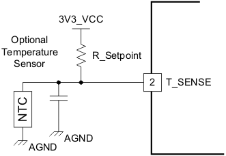 Figure 6. Negative Temperature Coefficient (NTC) Application
7.3.6 Fault Handling and Indication
The following is a table of End Power Transfer (EPT) packet responses, fault conditions, the duration how long the condition lasts until a retry in attempted. The LED mode selected determines how the LED indicates the condition or fault.
Table 3. Fault Handling and Indication
| CONDITION | DURATION (before retry) |
HANDLING |
|---|---|---|
| EPT-00 | Immediate | Unknown |
| EPT-01 | 5 seconds | Charge complete |
| EPT-02 | Infinite | Internal fault |
| EPT-03 | 5 minutes | Over temperature |
| EPT-04 | Immediate | Over voltage |
| EPT-05 | Immediate | Over current |
| EPT-06 | Infinite | Battery failure |
| EPT-07 | Not applicable | Reconfiguration |
| EPT-08 | Immediate | No response |
| OVP (over voltage) | Immediate | |
| OC (over current) | 1 minute | |
| NTC (external sensor) | 5 minutes | |
| PMOD/FOD warning | 12 seconds | 10 seconds LED only, 2 seconds LED + buzzer |
| PMOD/FOD | 5 minutes |
7.3.7 Power Transfer Start Signal
The bq500211A features two signal outputs to indicate that power transfer has begun. Pin 23 outputs a 400-ms duration, 4-kHz square wave for driving low cost AC type ceramic buzzers. Pin 24 outputs logic high, also for 400 ms, which is suitable for DC type buzzers with built-in tone generators, or as a trigger for any type of customized indication scheme. If not used, these pins can be left open.
7.3.8 Power-On Reset
The bq500211A has an integrated Power-On Reset (POR) circuit which monitors the supply voltage and handles the correct device startup sequence. Additional supply voltage supervisor or reset circuits are not needed.
7.3.9 External Reset, RESET Pin
The bq500211A can be forced into a reset state by an external circuit connected to the RESET pin. A logic low voltage on this pin holds the device in reset. For normal operation, this pin is pulled up to 3.3 VCC with a 10-kΩ pull-up resistor.
7.3.10 Trickle Charge and CS100
The WPC specification provides an End-of-Power Transfer message (EPT–01) to indicate charge complete. Upon receipt of the charge complete message, the bq500211A will change the LED indication to solid green LED output and halt power transfer for 5 seconds.
In some battery charging applications there is a benefit to continue the charging process in trickle-charge mode to top off the battery. There are several information packets in the WPC specification related to the levels of battery charge (Charge Status). The bq500211A uses these commands to enable top-off charging. The bq500211A changes the LED indication to reflect charge complete when a Charge Status message is 100% received, but unlike the response to an EPT, it will not halt power transfer while the LED is solid green. The mobile device can use a CS100 packet to enable trickle charge mode.
If the reported charge status drops below 90% normal, charging indication will be resumed.
7.3.11 Current Monitoring Requirements
The bq500211A is WPC1.1 ready. In order to enable the PMOD or FOD features, current monitoring must be provided in the design.
Current monitoring is optional however, it is used for the foreign metal protection features and over current protection. The system designer can choose not to include the current monitor and remain WPC1.0 compliant. Alternately, the additional current monitoring circuitry can be added to the hardware design but not loaded. This would enable a forward migration path to future WPC1.1 compatibility.
For proper scaling of the current monitor signal, the current sense resistor should be 20 mΩ and the current shunt amplifier should have a gain of 50, such as the INA199A1. The current sense resistor has a temperature stability of ±200 PPM. Proper current sensing techniques in the application hardware should also be observed.
7.3.12 Overcurrent Protection
The bq500211A has an integrated current protection feature which monitors the input current reported by the current sense resistor and amplifier. If the input current exceeds a safety threshold, a fault is indicated and power transfer is halted for one minute.
If this feature is desired, the sense resistor and amplifier are required. If this feature is not desired, the I_SENSE input pin to the bq500410A (pin 42) should be grounded.
NOTE
Always terminate the I_SENSE pin (pin 42), either with the output of a current monitor circuit or by connecting to ground.
7.3.13 MSP430G2001 Low Power Supervisor
This is an optional low-power feature. By adding the MSP430G2001, the entire bq500211A is periodically shut down to conserve power, yet all relevant states are recalled and all running LED status indicators remain on.
7.3.13.1 MSP430 Low Power Supervisor Details
Since the bq500211A needs an external low-power mode to significantly reduce power consumption, one way of positively achieving that goal is to remove its supply and completely shut it down. In doing so, however, the bq500211A goes through a reset and any data in memory would be lost. Important information regarding charge state, fault condition and operating mode would be cleared. The MSP430G2001 maintains the LED indication and stores previous charge state during the bq500211A reset period.
The LEDs indicators are now driven by the MSP430G2001, do not exceed the pin output current drive limit.
Using the suggested circuitry, a standby power reduction from 300 mW to less than 90 mW can be expected making it possible to achieve Energy Star rating.
The user does not need to program the MSP430G2001, an off-the-shelf part and any of the available packages can be used as long as the connections are correct. The required MSP430G2001 firmware is embedded in the bq500211A and is boot loaded at first power up, similar to a field update. The MSP430G2001 code cannot be modified by the user.
NOTE
The user cannot program the MSP430G2001 in this system.
7.3.14 All Unused Pins
All unused pins can be left open unless otherwise indicated. Pins 1, 3, 45 can be tied to GND and flooded with copper to improve ground shielding. Please refer to the pin definition table for further explanations.