SLUSBB1B December 2012 – June 2016
- 1 Features
- 2 Applications
- 3 Description
- 4 Revision History
- 5 Pin Configuration and Functions
- 6 Specifications
-
7 Detailed Description
- 7.1 Overview
- 7.2 Functional Block Diagram
- 7.3
Feature Description
- 7.3.1 Dynamic Power Limiting™
- 7.3.2 Option Select Pin
- 7.3.3 LED Indication Modes
- 7.3.4 Parasitic Metal Object Detect (PMOD) and Foreign Object Detection (FOD)
- 7.3.5 Shut Down via External Thermal Sensor or Trigger
- 7.3.6 Fault Handling and Indication
- 7.3.7 Power Transfer Start Signal
- 7.3.8 Power-On Reset
- 7.3.9 External Reset, RESET Pin
- 7.3.10 Trickle Charge and CS100
- 7.3.11 Current Monitoring Requirements
- 7.3.12 Overcurrent Protection
- 7.3.13 MSP430G2001 Low Power Supervisor
- 7.3.14 All Unused Pins
- 8 Application and Implementation
- 9 Layout
- 10Device and Documentation Support
- 11Mechanical, Packaging, and Orderable Information
Package Options
Mechanical Data (Package|Pins)
- RGZ|48
Thermal pad, mechanical data (Package|Pins)
- RGZ|48
Orderable Information
8 Application and Implementation
NOTE
Information in the following applications sections is not part of the TI component specification, and TI does not warrant its accuracy or completeness. TI’s customers are responsible for determining suitability of components for their purposes. Customers should validate and test their design implementation to confirm system functionality.
8.1 Typical Application
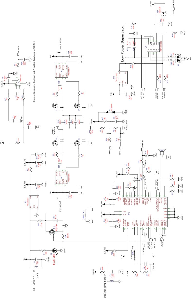
The application schematic for the transmitter with reduced standby power is shown in Figure 7.
CAUTION
Please check the bq500211A product page for the most up-to-date application schematic and list of materials package before starting a new design.
 Figure 7. bq500211A Typical Low-Standby Power Application Diagram
8.1.1 Detailed Design Procedure
8.1.1.1 Coils and Matching Capacitors
The coil and matching capacitor selection for the transmitter has been established by WPC standard. This is fixed and cannot be changed on the transmitter side.
An up to date list of available and compatible A5 and A11 transmitter coils can be found here (SLUA649):
Capacitor selection is critical to proper system operation. A total capacitance value of 400 nF is required in the resonant tank. This is the WPC system compatibility requirement, not a guideline, and must be followed.
NOTE
A total capacitance value of 400 nF/50 V (C0G dielectric type or equivalent) is required in the resonant tank to achieve a 100-kHz resonance frequency.
The capacitors chosen must be rated for at least 50 V and must be of high quality C0G dielectric or equivalent. These are typically available in a 5% tolerance. The use of X7R types or below is not recommended if WPC compliance is required because critical WPC certification testing, such as the minimum modulation requirement, might fail.
A 400-nF capacitor is not a standard value and therefore several must be combined in parallel. The designer can combine a (4 nF x 100 nF) or a (180 nF + 220 nF) along with other combinations depending on market availability. All capacitors must be of high quality C0G type or equivalent and not mixed with lesser dielectric types.
8.1.1.2 Input Regulator
The bq500211A requires 3.3 VDC to operate. A buck regulator or a linear regulator can be used to step down from the 5-V system input. Either choice is fully WPC compatible, the decision lies in the user's requirements with respect to cost or efficiency.
For highest efficiency use a low-cost buck regulator, TPS62237, which on account of a 3-MHz switching frequency, can use a 0805 size chip inductor. This results in a very attractive combination, high performance, small size, ease of use and low cost.
8.1.1.3 Power Train
The bq500211A drives a phase-shifted full bridge. This is essentially twin half bridges and the choice of driver devices is quite simple, a pair of TPS28225 synchronous MOSFET drivers are used with four CSD17308Q2 NexFETs. Other combinations work and system performance with regards to efficiency and EMI emissions vary. Any alternate MOSFETs chosen must be fully saturated at 5-V gate drive and be sure to pay attention whether or not to use gate resistors; some tuning might be required.
8.1.1.4 Low Power Supervisor
Power reduction is achieved by periodically disabling the bq500211A while LED and housekeeping control functions are continued by U4 – the low-cost, low quiescent current microcontroller MSP430G2001. When U4 is present in the circuit (which is set by a pull-up resistor on bq500211A pin 25), the bq500211A at first power-up boots the MSP430G2001 with the necessary firmware and the two chips operate in tandem. During standby operation, the bq500211A periodically issues a SLEEP command, Q12 pulls the RESET pin low, therefore reducing its power consumption. Meanwhile, the MSP430G2001 maintains the LED indication and stores previous charge state during this bq500211A reset period. This bq500211A reset period is set by the RC time constant network of R26, C22 (see Figure 7). WPC compliance mandates receive detection within 500 ms, the power transmitter controller, bq500211A, awakes every 400 ms to produce an analog ping and check if a valid device is present. Increasing this time constant, therefore is not advised; shortening could result in faster detection time with some decrease in efficiency.
8.1.1.5 Disabling Low Power Supervisor Mode
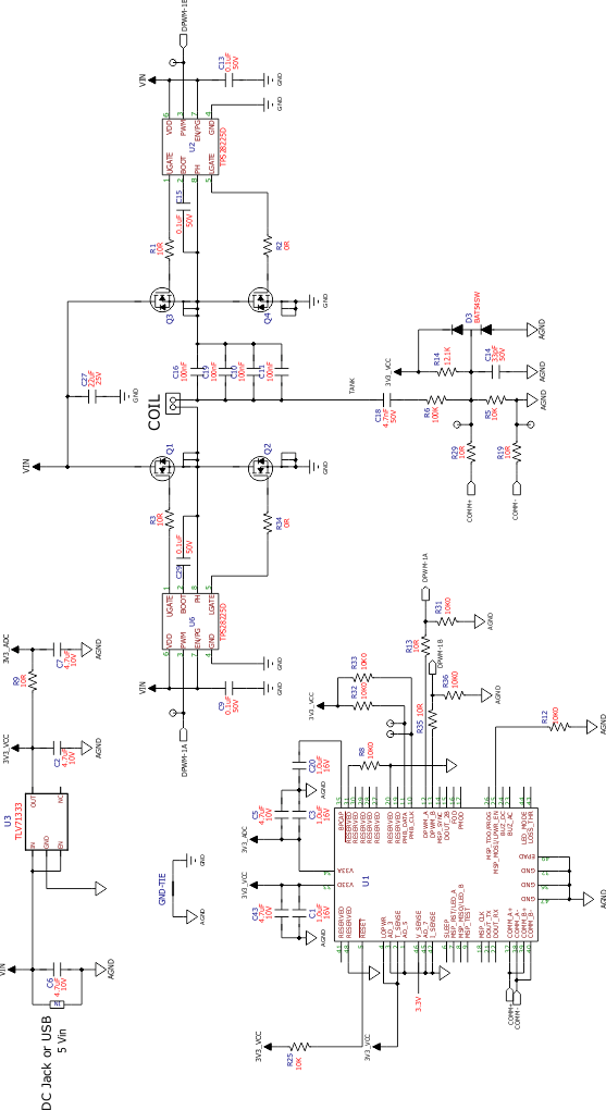
For lowest cost or if the low-power supervisor is not needed, please refer to Figure 8 for the application schematic.
NOTE
Current sense shunt and amplifier circuitry are optional. The circuitry is needed to enable Foreign Object Detection (FOD) and a forward migration path to WPC1.1 compliance.
