SLUSBC8C December 2013 – July 2018
PRODUCTION DATA.
- 1 Features
- 2 Applications
- 3 Description
- 4 Revision History
- 5 Device Comparison Table
- 6 Pin Configuration and Functions
- 7 Specifications
-
8 Detailed Description
- 8.1 Overview
- 8.2 Functional Block Diagram
- 8.3
Feature Description
- 8.3.1 Details of a Qi Wireless Power System and bq51003 Power Transfer Flow Diagrams
- 8.3.2 Dynamic Rectifier Control
- 8.3.3 Dynamic Efficiency Scaling
- 8.3.4 RILIM Calculations
- 8.3.5 Input Overvoltage
- 8.3.6 Adapter Enable Functionality and EN1/EN2 Control
- 8.3.7 End Power Transfer Packet (WPC Header 0x02)
- 8.3.8 Status Outputs
- 8.3.9 WPC Communication Scheme
- 8.3.10 Communication Modulator
- 8.3.11 Adaptive Communication Limit
- 8.3.12 Synchronous Rectification
- 8.3.13 Temperature Sense Resistor Network (TS)
- 8.3.14 3-State Driver Recommendations for the TS-CTRL Pin
- 8.3.15 Thermal Protection
- 8.3.16 WPC v1.2 Compliance – Foreign Object Detection
- 8.4 Device Functional Modes
- 9 Application and Implementation
- 10Power Supply Recommendations
- 11Layout
- 12Device and Documentation Support
- 13Mechanical, Packaging, and Orderable Information
Package Options
Mechanical Data (Package|Pins)
- YFP|28
Thermal pad, mechanical data (Package|Pins)
Orderable Information
9.2.2.3 Application Curves
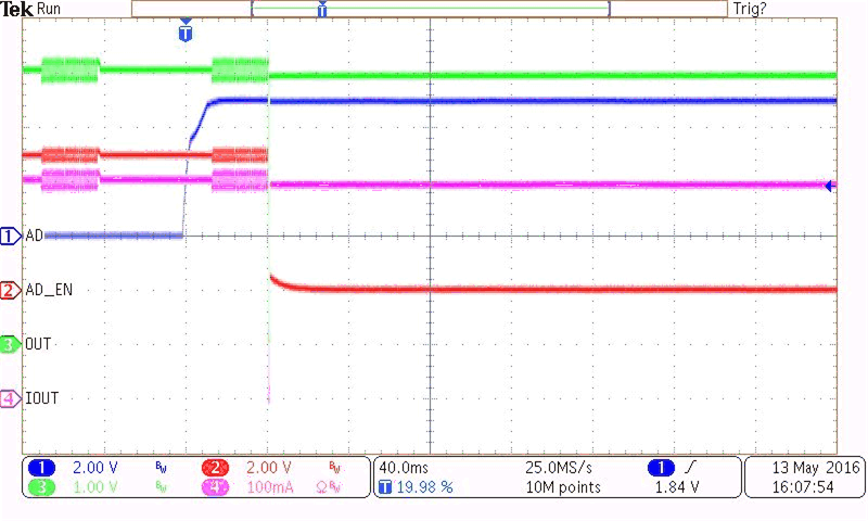
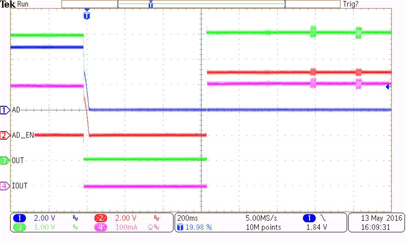
The following figures show the bq51003EVM-764 when DC voltage is applied to the AD pin and when it is removed. The AD pin signal shows when the DC power is applied or removed. The AD_EN signal shows the response of to the added or removed power on the AD pin. The OUT pin signal shows the impact to the OUT pin during the AD addition or removal. IOUT shows the current being sourced by the OUT pin. The resistive load is set to produce 400 mA at 5 V. On both of the following plots, note the communication packets are not present when AD_EN is low.
Figure 39 shows the bq51003EVM-764 when a power source is added to the AD pin. The bq51003 disables the OUT pin then sets AD_EN to low which enables the CSD75207W15, passing the DC voltage to the load.
Figure 40 shows the response when the DC voltage is removed. Note the time after the removal before OUT is enabled which allows the bq51003 to communicate with the transmitter to get RECT back to the correct level.
 Figure 39. DC Voltage is Added at AD
  Figure 40. DC Voltage is Removed from AD