SWRS187D August 2016 – July 2019 CC2650MODA
PRODUCTION DATA.
- 1 Device Overview
- 2 Revision History
- 3 Device Comparison
- 4 Terminal Configuration and Functions
-
5 Specifications
- 5.1 Absolute Maximum Ratings
- 5.2 ESD Ratings
- 5.3 Recommended Operating Conditions
- 5.4 Power Consumption Summary
- 5.5 General Characteristics
- 5.6 Antenna
- 5.7 1-Mbps GFSK (Bluetooth low energy) – RX
- 5.8 1-Mbps GFSK (Bluetooth low energy) – TX
- 5.9 IEEE 802.15.4 (Offset Q-PSK DSSS, 250 kbps) – RX
- 5.10 IEEE 802.15.4 (Offset Q-PSK DSSS, 250 kbps) – TX
- 5.11 24-MHz Crystal Oscillator (XOSC_HF)
- 5.12 32.768-kHz Crystal Oscillator (XOSC_LF)
- 5.13 48-MHz RC Oscillator (RCOSC_HF)
- 5.14 32-kHz RC Oscillator (RCOSC_LF)
- 5.15 ADC Characteristics
- 5.16 Temperature Sensor
- 5.17 Battery Monitor
- 5.18 Continuous Time Comparator
- 5.19 Low-Power Clocked Comparator
- 5.20 Programmable Current Source
- 5.21 DC Characteristics
- 5.22 Thermal Resistance Characteristics for MOH Package
- 5.23 Timing Requirements
- 5.24 Switching Characteristics
- 5.25 Typical Characteristics
-
6 Detailed Description
- 6.1 Overview
- 6.2 Functional Block Diagram
- 6.3 Main CPU
- 6.4 RF Core
- 6.5 Sensor Controller
- 6.6 Memory
- 6.7 Debug
- 6.8 Power Management
- 6.9 Clock Systems
- 6.10 General Peripherals and Modules
- 6.11 System Architecture
- 6.12 Certification
- 6.13 End Product Labeling
- 6.14 Manual Information to the End User
- 6.15 Module Marking
- 7 Application, Implementation, and Layout
- 8 Environmental Requirements and Specifications
- 9 Device and Documentation Support
- 10Mechanical, Packaging, and Orderable Information
Package Options
Refer to the PDF data sheet for device specific package drawings
Mechanical Data (Package|Pins)
- MOH|29
Thermal pad, mechanical data (Package|Pins)
Orderable Information
7.2.1 Layout Guidelines
Use the following guidelines to lay out the CC2650MODA device:
- The module must be placed close to the edge of the PCB.
- TI recommends leaving copper clearance on all PCB layers underneath the antenna area, as shown in Figure 7-2 and Figure 7-3.
- TI recommends using a generous amount of ground vias to stitch together the ground planes on different layers. Several ground vias should be placed close to the exposed ground pads of the module.
- No external decoupling is required.
- The reset line should have an external pullup resistor unless the line is actively driven. Placement of this component is not critical.
- TI recommends leaving a clearance in the top-side copper plane underneath the RF test pads.
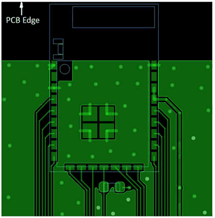 Figure 7-2 Top Layer
 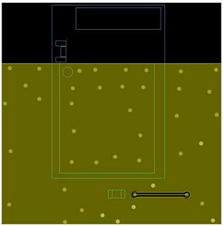 Figure 7-3 Bottom Layer