SWRS187D August 2016 – July 2019 CC2650MODA
PRODUCTION DATA.
- 1 Device Overview
- 2 Revision History
- 3 Device Comparison
- 4 Terminal Configuration and Functions
-
5 Specifications
- 5.1 Absolute Maximum Ratings
- 5.2 ESD Ratings
- 5.3 Recommended Operating Conditions
- 5.4 Power Consumption Summary
- 5.5 General Characteristics
- 5.6 Antenna
- 5.7 1-Mbps GFSK (Bluetooth low energy) – RX
- 5.8 1-Mbps GFSK (Bluetooth low energy) – TX
- 5.9 IEEE 802.15.4 (Offset Q-PSK DSSS, 250 kbps) – RX
- 5.10 IEEE 802.15.4 (Offset Q-PSK DSSS, 250 kbps) – TX
- 5.11 24-MHz Crystal Oscillator (XOSC_HF)
- 5.12 32.768-kHz Crystal Oscillator (XOSC_LF)
- 5.13 48-MHz RC Oscillator (RCOSC_HF)
- 5.14 32-kHz RC Oscillator (RCOSC_LF)
- 5.15 ADC Characteristics
- 5.16 Temperature Sensor
- 5.17 Battery Monitor
- 5.18 Continuous Time Comparator
- 5.19 Low-Power Clocked Comparator
- 5.20 Programmable Current Source
- 5.21 DC Characteristics
- 5.22 Thermal Resistance Characteristics for MOH Package
- 5.23 Timing Requirements
- 5.24 Switching Characteristics
- 5.25 Typical Characteristics
-
6 Detailed Description
- 6.1 Overview
- 6.2 Functional Block Diagram
- 6.3 Main CPU
- 6.4 RF Core
- 6.5 Sensor Controller
- 6.6 Memory
- 6.7 Debug
- 6.8 Power Management
- 6.9 Clock Systems
- 6.10 General Peripherals and Modules
- 6.11 System Architecture
- 6.12 Certification
- 6.13 End Product Labeling
- 6.14 Manual Information to the End User
- 6.15 Module Marking
- 7 Application, Implementation, and Layout
- 8 Environmental Requirements and Specifications
- 9 Device and Documentation Support
- 10Mechanical, Packaging, and Orderable Information
Package Options
Refer to the PDF data sheet for device specific package drawings
Mechanical Data (Package|Pins)
- MOH|29
Thermal pad, mechanical data (Package|Pins)
Orderable Information
5.25 Typical Characteristics
This section contains typical performance plots measured on the CC2650F128RHB device. They are published in the CC2650 data sheet, and the plots relevant for the CC2650MODA device are repeated here. RF performance is specified in a single-ended 50-Ω reference plane at the antenna feeding point with Tc = 25°C and VDD = 3.0 V, unless otherwise noted.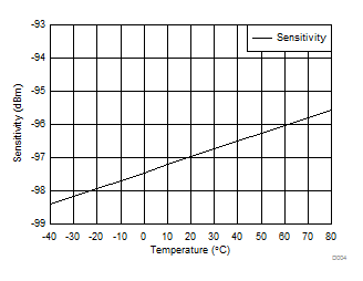 Figure 5-4 Bluetooth low energy Sensitivity vs Temperature
 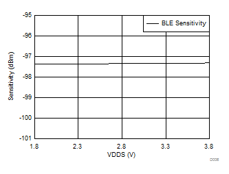 Figure 5-6 Bluetooth low energy Sensitivity
vs Supply Voltage (VDD)
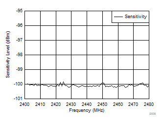 Figure 5-8 IEEE 802.15.4 Sensitivity
vs Channel Frequency
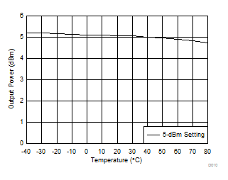 Figure 5-10 TX Output Power vs Temperature
 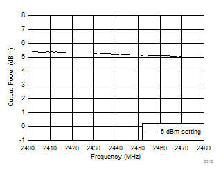 Figure 5-12 TX Output Power
vs Channel Frequency
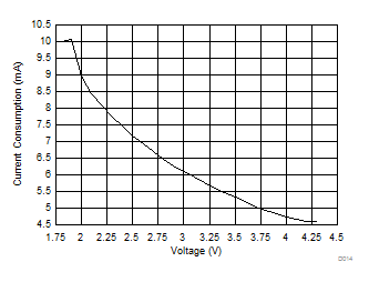 Figure 5-14 RX Mode Current vs Supply Voltage (VDD)
 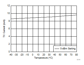 Figure 5-16 TX Mode Current Consumption vs Temperature
 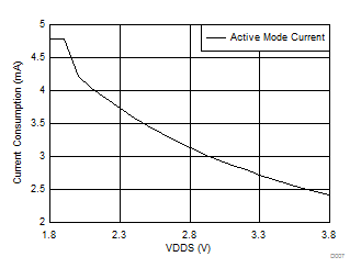 Figure 5-18 Active Mode (MCU Running, No Peripherals)
Current Consumption vs Supply Voltage (VDD)
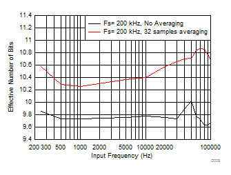 Figure 5-20 SoC ADC Effective Number of Bits vs Input Frequency (Internal Reference)
 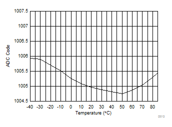 Figure 5-22 SoC ADC Output vs Temperature (Fixed Input, Internal Reference)
 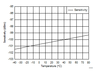 Figure 5-5 IEEE 802.15.4 Sensitivity vs Temperature
 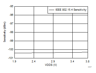 Figure 5-7 IEEE 802.15.4 Sensitivity
vs Supply Voltage (VDD)
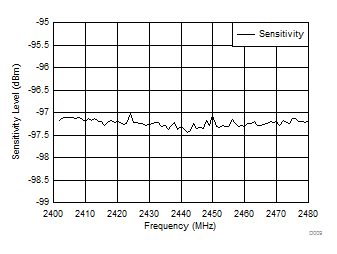 Figure 5-9 Bluetooth low energy Sensitivity
vs Channel Frequency
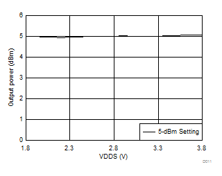 Figure 5-11 TX Output Power vs Supply Voltage (VDD)
 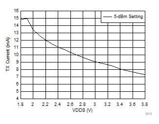 Figure 5-13 TX Current Consumption
vs Supply Voltage (VDD)
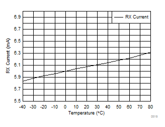 Figure 5-15 RX Mode Current Consumption vs Temperature
 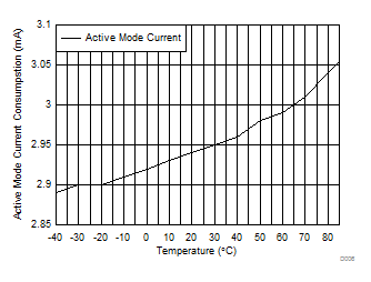 Figure 5-17 Active Mode (MCU Running, No Peripherals)
Current Consumption vs Temperature
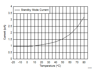 Figure 5-19 Standby Mode Current Consumption
With RCOSC RTC vs Temperature
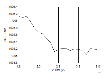 Figure 5-21 SoC ADC Output vs Supply Voltage (Fixed Input, Internal Reference)
 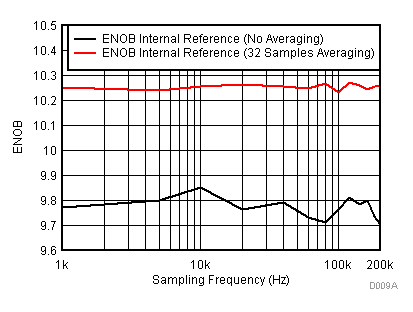 Figure 5-23 SoC ADC ENOB vs Sampling Frequency
(Input Frequency = FS / 10)
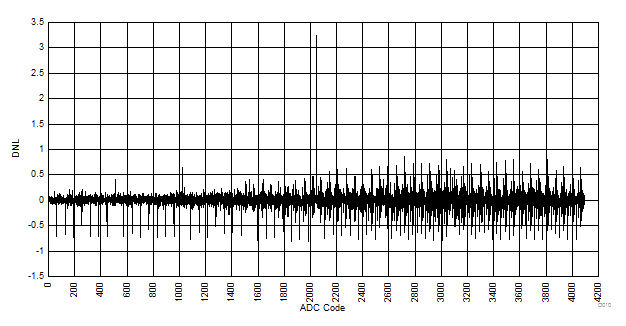 Figure 5-24 SoC ADC DNL vs ADC Code (Internal Reference)
 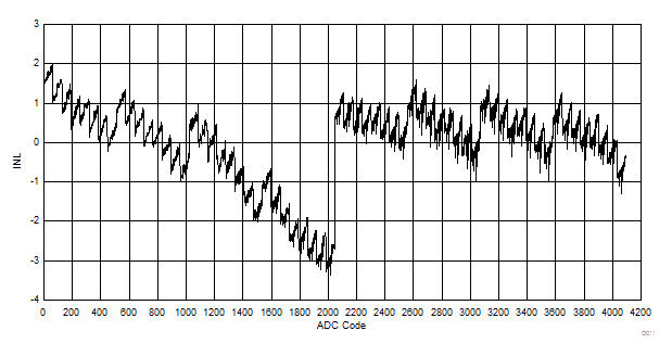 Figure 5-25 SoC ADC INL vs ADC Code (Internal Reference)