SCLS464A September 2002 – January 2015 CD74HC4051-EP
PRODUCTION DATA.
- 1 Features
- 2 Applications
- 3 Description
- 4 Revision History
- 5 Pin Configuration And Functions
- 6 Specifications
- 7 Parameter Measurement Information
- 8 Detailed Description
- 9 Application and Implementation
- 10Power Supply Recommendations
- 11Layout
- 12Device And Documentation Support
- 13Mechanical, Packaging, and Orderable Information
Package Options
Refer to the PDF data sheet for device specific package drawings
Mechanical Data (Package|Pins)
- D|16
Thermal pad, mechanical data (Package|Pins)
Orderable Information
8 Detailed Description
8.1 Overview
The CD74HC4051-EP is a digitally controlled analog switch that uses silicon gate CMOS technology to achieve operating speeds similar to LSTTL, with the low-power consumption of standard CMOS integrated circuits.
8.2 Functional Block Diagram
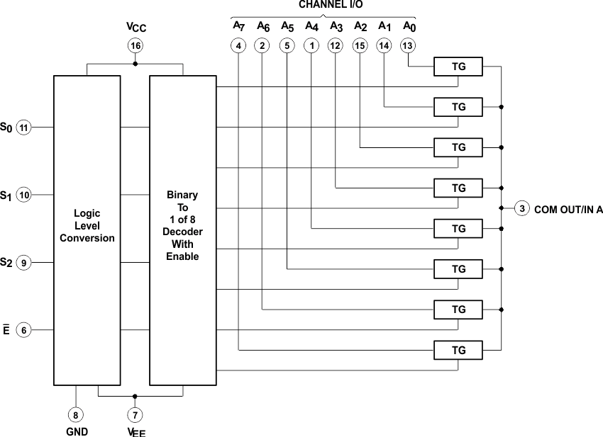
8.3 Feature Description
This analog multiplexer and demultiplexer controls analog voltages that may vary across the voltage supply range (that is, VCC to VEE). These bidirectional switches allow the use of any analog input as an output and vice versa. The switches have low ON-resistance and low OFF leakages. In addition, the device has an enable control (E) that, when high, disables all switches to their OFF state.
8.4 Device Functional Modes
Table 1. Function Table
| INPUTS | ON CHANNEL (S) |
|||
|---|---|---|---|---|
| E | S2 | S1 | S0 | |
| L L L L L L L L H |
L L L L H H H H X |
L L H H L L H H X |
L H L H L H L H X |
A0 A1 A2 A3 A4 A5 A6 A7 None |
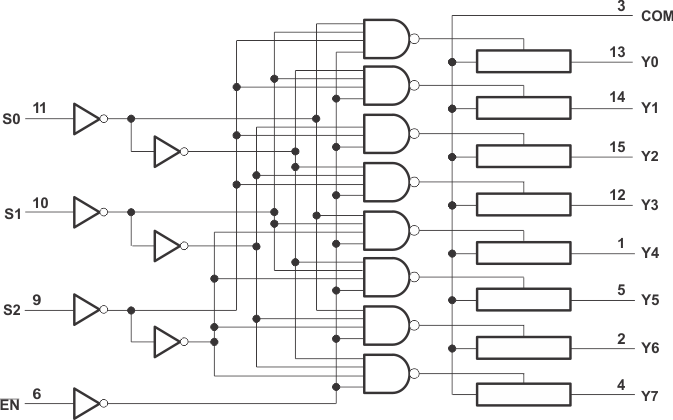 Figure 10. Logic Diagram (Positive Logic)