SCHS279E December 1998 – August 2022 CD54HC4511 , CD74HC4511 , CD74HCT4511
PRODUCTION DATA
- 1 Features
- 2 Description
- 3 Revision History
- 4 Pin Configuration and Functions
-
5 Specifications
- 5.1 Absolute Maximum Ratings
- 5.2 Recommended Operating Conditions for 'HC4511 (1)
- 5.3 Recommended Operating Conditions for CD74HCT4511 (1)
- 5.4 Thermal Information
- 5.5 'HC4511 Electrical Characteristics
- 5.6 CD74HCT4511 Electrical Characteristics
- 5.7 'HC4511 Timing Requirements
- 5.8 Switching Characteristics
- 5.9 CD74HCT4511 Timing Requirements
- 5.10 CD74HCT4511 Switching Characteristics
- 5.11 Operating Characteristics
- 6 Parameter Measurement Information
- 7 Detailed Description
- 8 Power Supply Recommendations
- 9 Layout
- 10Device and Documentation Support
- 11Mechanical, Packaging, and Orderable Information
Package Options
Refer to the PDF data sheet for device specific package drawings
Mechanical Data (Package|Pins)
- PW|16
- N|16
- D|16
Thermal pad, mechanical data (Package|Pins)
Orderable Information
2 Description
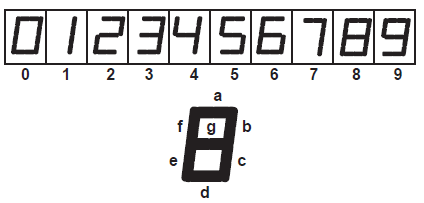
The CD54HC4511, CD74HC4511, and CD74HCT4511 are BCD-to-7 segment latch/decoder/drivers with four address inputs (D0−D3), an active-low blanking (BL) input, lamp-test (LT) input, and a latch-enable (LE) input that, when high, enables the latches to store the BCD inputs. When LE is low, the latches are disabled, making the outputs transparent to the BCD inputs.
Device Information
| PART NUMBER | PACKAGE(1) | BODY SIZE (NOM) |
|---|---|---|
| CD54HC4511 | J (CDIP, 16) | 24.38 mm × 6.92 mm |
| CD74HC4511 | N (PDIP, 16) | 19.31 mm × 6.35 mm |
| D (SOIC, 16) | 9.90 mm × 3.90 mm | |
| PW (TSSOP, 16) | 5.00 mm × 4.40 mm | |
| CD74HCT4511 | N (PDIP, 16) | 19.31 mm × 6.35 mm |
(1) For all available packages, see
the orderable addendum at the end of the data sheet.
 Display