SNAS787A November 2019 – February 2020 CDCDB2000
PRODUCTION DATA.
- 1 Features
- 2 Applications
- 3 Description
- 4 Revision History
- 5 Pin Configuration and Functions
- 6 Specifications
-
7 Detailed Description
- 7.1 Overview
- 7.2 Functional Block Diagram
- 7.3 Feature Description
- 7.4 Device Functional Modes
- 7.5 Programming
- 7.6
Register Maps
- 7.6.1
CDCDB2000 Registers
- 7.6.1.1 OECR1 Register (Address = 0h) [reset = 78h]
- 7.6.1.2 OECR2 Register (Address = 1h) [reset = FFh]
- 7.6.1.3 OECR3 Register (Address = 2h) [reset = FFh]
- 7.6.1.4 OERDBK Register (Address = 3h) [reset = 0h]
- 7.6.1.5 SBRDBK Register (Address = 4h) [reset = 1h]
- 7.6.1.6 VDRREVID Register (Address = 5h) [reset = X]
- 7.6.1.7 DEVID Register (Address = 6h) [reset = X]
- 7.6.1.8 BTRDCNT Register (Address = 7h) [reset = 8h]
- 7.6.1.9 SBIMSK1 Register (Address = 8h) [reset = 0h]
- 7.6.1.10 SBIMSK2 Register (Address = 9h) [reset = 0h]
- 7.6.1.11 SBIMSK3 Register (Address = Ah) [reset = 0h]
- 7.6.1
CDCDB2000 Registers
- 8 Application and Implementation
- 9 Power Supply Recommendations
- 10Layout
- 11Device and Documentation Support
- 12Mechanical, Packaging, and Orderable Information
Package Options
Mechanical Data (Package|Pins)
- NPP|80
Thermal pad, mechanical data (Package|Pins)
Orderable Information
7.4.1 CKPWRGD_PD# Function
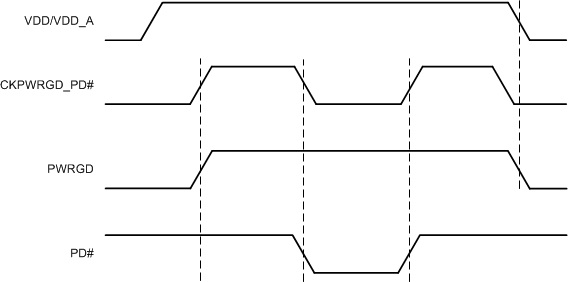
The CKPWRGD_PD# pin is used to set 2 state variables inside of the device: PWRGD, and PD#. The PWRGD and PD# variables control which functions of the device are active at any time, as well as the state of the input and output pins.
The PWRGD and PD# states are multiplexed on the CKPWRGD_PD# pin. CKPWRGD_PD# must remain below VOL and not exceed VDD_A + 0.3 V until VDD, VDD_A, and CLKIN are present and within the recommended operating conditions.
The first rising edge of the CKPWRGD_PD# pin sets PWRGD = 1. After PWRGD is set to 1, the CKPWRGD_PD# pin is used to assert PD# mode only. PWRGD variable will only be cleared to 0 with the removal of VDD and VDD_A.
 Figure 6. PWRGD and PD# State Changes