SNAS787A November   2019  – February 2020 CDCDB2000

PRODUCTION DATA.  

  1. Features
  2. Applications
  3. Description
    1.     Device Images
      1.      CDCDB2000 System Diagram
  4. Revision History
  5. Pin Configuration and Functions
    1.     Pin Functions
  6. Specifications
    1. Table 1. Absolute Maximum Ratings
    2. Table 2. ESD Ratings
    3. Table 3. Recommended Operating Conditions
    4. Table 4. Thermal Information
    5. Table 5. Electrical Characteristics
    6. Table 6. Timing Requirements
    7. 6.1      Typical Characteristics
  7. Detailed Description
    1. 7.1 Overview
    2. 7.2 Functional Block Diagram
    3. 7.3 Feature Description
      1. 7.3.1 Output Enable Control
      2. 7.3.2 SMBus
        1. 7.3.2.1 SMBus Address Assignment
      3. 7.3.3 Side-Band Interface
    4. 7.4 Device Functional Modes
      1. 7.4.1 CKPWRGD_PD# Function
      2. 7.4.2 OE[12:5]# and SMBus Output Enables
    5. 7.5 Programming
      1. 7.5.1 SMBus
      2. 7.5.2 SBI
    6. 7.6 Register Maps
      1. 7.6.1 CDCDB2000 Registers
        1. 7.6.1.1  OECR1 Register (Address = 0h) [reset = 78h]
          1. Table 11. OECR1 Register Field Descriptions
        2. 7.6.1.2  OECR2 Register (Address = 1h) [reset = FFh]
          1. Table 12. OECR2 Register Field Descriptions
        3. 7.6.1.3  OECR3 Register (Address = 2h) [reset = FFh]
          1. Table 13. OECR3 Register Field Descriptions
        4. 7.6.1.4  OERDBK Register (Address = 3h) [reset = 0h]
          1. Table 14. OERDBK Register Field Descriptions
        5. 7.6.1.5  SBRDBK Register (Address = 4h) [reset = 1h]
          1. Table 15. SBRDBK Register Field Descriptions
        6. 7.6.1.6  VDRREVID Register (Address = 5h) [reset = X]
          1. Table 16. VDRREVID Register Field Descriptions
        7. 7.6.1.7  DEVID Register (Address = 6h) [reset = X]
          1. Table 17. DEVID Register Field Descriptions
        8. 7.6.1.8  BTRDCNT Register (Address = 7h) [reset = 8h]
          1. Table 18. BTRDCNT Register Field Descriptions
        9. 7.6.1.9  SBIMSK1 Register (Address = 8h) [reset = 0h]
          1. Table 19. SBIMSK1 Register Field Descriptions
        10. 7.6.1.10 SBIMSK2 Register (Address = 9h) [reset = 0h]
          1. Table 20. SBIMSK2 Register Field Descriptions
        11. 7.6.1.11 SBIMSK3 Register (Address = Ah) [reset = 0h]
          1. Table 21. SBIMSK3 Register Field Descriptions
  8. Application and Implementation
    1. 8.1 Application Information
    2. 8.2 Typical Application
      1. 8.2.1 Design Requirements
      2. 8.2.2 Detailed Design Procedure
        1. 8.2.2.1 Output Enable Control Method
        2. 8.2.2.2 SMBus Address
      3. 8.2.3 Application Curve
  9. Power Supply Recommendations
  10. 10Layout
    1. 10.1 Layout Guidelines
    2. 10.2 Layout Examples
  11. 11Device and Documentation Support
    1. 11.1 Device Support
      1. 11.1.1 TICS Pro
    2. 11.2 Receiving Notification of Documentation Updates
    3. 11.3 Support Resources
    4. 11.4 Trademarks
    5. 11.5 Electrostatic Discharge Caution
    6. 11.6 Glossary
  12. 12Mechanical, Packaging, and Orderable Information

Package Options

Mechanical Data (Package|Pins)
Thermal pad, mechanical data (Package|Pins)
Orderable Information

Typical Application

Figure 10 shows a CDCDB2000 typical application. In this application, a clock generator provides a 100-MHz reference to the CDCDB2000 which then distributes that clock to PCIe endpoints. The clock generator may be a discrete clock generator like the LMK03328 or it may be integrated in a larger component such as a PCH or application processor.
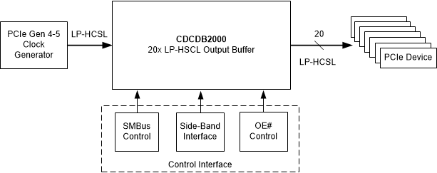
CDCDB2000 fbd-02-snas787.gifFigure 10. Typical Application