SNAS818B July 2021 – May 2022 CDCDB800
PRODUCTION DATA
- 1 Features
- 2 Applications
- 3 Description
- 4 Revision History
- 5 Pin Configuration and Functions
- 6 Specifications
- 7 Parameter Measurement Information
- 8 Detailed Description
- 9 Application and Implementation
- 10Power Supply Recommendations
- 11Layout
- 12Device and Documentation Support
- 13Mechanical, Packaging, and Orderable Information
Package Options
Mechanical Data (Package|Pins)
- RSL|48
Thermal pad, mechanical data (Package|Pins)
- RSL|48
Orderable Information
10 Power Supply Recommendations
High-performance clock buffers are sensitive to noise on the power supply, which can dramatically increase the additive jitter of the buffer. Thus, it is essential to reduce noise from the system power supply, especially when the jitter and phase noise is critical to applications.
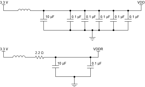
Filter capacitors are used to eliminate the low-frequency noise from the power supply, where the bypass capacitors provide the very low impedance path for high-frequency noise and guards the power-supply system against induced fluctuations. These bypass capacitors also provide instantaneous current surges as required by the device and should have low equivalent series resistance (ESR). To properly use the bypass capacitors, place the capacitors very close to the power-supply terminals and lay out with short loops to minimize inductance. TI recommends to insert a ferrite bead between the board power supply and the chip power supply that isolates the high-frequency switching noises generated by the clock buffer. These beads prevent the switching noise from leaking into the board supply. It is imperative to choose an appropriate ferrite bead with very low DC resistance to provide adequate isolation between the board supply and the chip supply, as well as to maintain a voltage at the supply terminals that is greater than the minimum voltage required for proper operation.
Figure 10-1 shows the recommended power supply filtering and decoupling method.
 Figure 10-1 Power Supply Decoupling