SNAS705D January 2017 – February 2024 CDCE813-Q1
PRODUCTION DATA
- 1
- 1 Features
- 2 Applications
- 3 Description
- 4 Pin Configuration and Functions
- 5 Specifications
- 6 Parameter Measurement Information
- 7 Detailed Description
- 8 Application and Implementation
- 9 Register Maps
- 10Device and Documentation Support
- 11Revision History
- 12Mechanical, Packaging, and Orderable Information
Package Options
Mechanical Data (Package|Pins)
- PW|14
Thermal pad, mechanical data (Package|Pins)
Orderable Information
3 Description
The CDCE813-Q1 device is a modular Phase-locked-loop-based (PLL), low-cost, high-performance, programmable clock synthesizers. They generate up to three output clocks from a single input frequency. Each output can be programmed in-system for any clock frequency up to 230MHz, using the integrated configurable PLL.
The CDCE813-Q1 has separate output supply pins, VDDOUT, providing 2.5V to 3.3V.
The input accepts an external crystal or LVCMOS clock signal. A selectable on-chip VCXO allows synchronization of the output frequency to an external control signal.
The PLL supports SSC (spread-spectrum clocking) for better electromagnetic interference (EMI) performance.
The device supports nonvolatile EEPROM programming for easy customization of the device to the application. All device settings are programmable through the I2C bus, a 2-wire serial interface.
The CDCE813-Q1 operates in a 1.8V core environment as well as eliminating the need for additional, independent XTAL oscillators which reduces component count and board size. The device operates in a temperature range of –40°C to 105°C.
| ORDERABLE | S0 CONTROL PIN DEFAULT FUNCTION |
|---|---|
| CDCE813R02-Q1 | Y1 Output Enable (Active High) |
| CDCE813-Q1 | Not Used(1) |
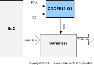
 Typical Application Schematic