SCAS901D September 2010 – November 2017 CDCLVD1212
PRODUCTION DATA.
- 1 Features
- 2 Applications
- 3 Description
- 4 Revision History
- 5 Pin Configuration and Functions
- 6 Specifications
- 7 Parameter Measurement Information
- 8 Detailed Description
- 9 Application and Implementation
- 10Power Supply Recommendations
- 11Layout
- 12Device and Documentation Support
- 13Mechanical, Packaging, and Orderable Information
Package Options
Mechanical Data (Package|Pins)
- RHA|40
Thermal pad, mechanical data (Package|Pins)
Orderable Information
9 Application and Implementation
NOTE
Information in the following applications sections is not part of the TI component specification, and TI does not warrant its accuracy or completeness. TI’s customers are responsible for determining suitability of components for their purposes. Customers should validate and test their design implementation to confirm system functionality.
9.1 Application Information
The CDCLVD1212 is a low additive jitter universal to LVDS fan-out buffer with 2 selectable inputs. The small package, low output skew, and low additive jitter make for a flexible device in demanding applications.
9.2 Typical Application
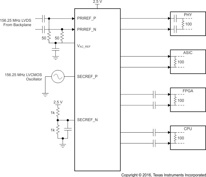
 Figure 16. Fan-Out Buffer for Line Card Application
9.2.1 Design Requirements
The CDCLVD1212 shown in Figure 16 is configured to select two inputs: a 156.25-MHz LVDS clock from the backplane, or a secondary 156.25-MHz LVCMOS 2.5-V oscillator. The LVDS clock is AC-coupled and biased using the integrated reference voltage generator. A resistor divider is used to set the threshold voltage correctly for the LVCMOS clock. 0.1-µF capacitors are used to reduce noise on both VAC_REF and SECREF_N. Either input signal can be then fanned out to desired devices, as shown. The configuration example is driving 4 LVDS receivers in a line card application with the following properties:
- The PHY device is capable of DC-coupling with an LVDS driver such as the CDCLVD1212. This PHY device features internal termination so no additional components are required for proper operation.
- The ASIC LVDS receiver features internal termination and operates at the same common-mode voltage as the CDCLVD1212. Again, no additional components are required.
- The FPGA requires external AC-coupling, but has internal termination. 0.1-µF capacitors are placed to provide AC-coupling. Similarly, the CPU is internally terminated, and requires only external AC-coupling capacitors.
- The unused outputs of the CDCLVD1212 are left floating.
9.2.2 Detailed Design Procedure
See Input Termination for proper input terminations, dependent on single-ended or differential inputs.
See LVDS Output Termination for output termination schemes depending on the receiver application.
Unused outputs can be left floating.
In this example, the PHY, ASIC, and FPGA or CPU require different schemes. Power supply filtering and bypassing is critical for low-noise applications.
See Power Supply Recommendations for recommended filtering techniques. A reference layout is provided in Low-Additive Jitter, Twelve LVDS Outputs Clock Buffer Evaluation Board (SCAU045).
9.2.3 Application Curves
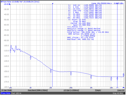
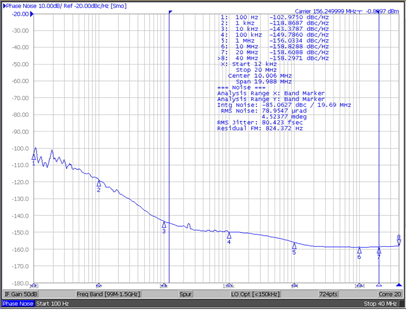
The CDCLVD12xx's low additive noise is shown in this line card application. The low noise 156.25-MHz source with 67-fs RMS jitter drives the CDCLVD12xx, resulting in 80-fs RMS when integrated from 12 kHz to 20 MHz. The resultant additive jitter is a low 44-fs RMS for this configuration.

| Reference signal is low-noise Rohde & Schwarz SMA100A |
67-fs RMS (12 kHz to 20 MHz)

80-fs RMS (12 kHz to 20 MHz)