SCAS901D September 2010 – November 2017 CDCLVD1212
PRODUCTION DATA.
- 1 Features
- 2 Applications
- 3 Description
- 4 Revision History
- 5 Pin Configuration and Functions
- 6 Specifications
- 7 Parameter Measurement Information
- 8 Detailed Description
- 9 Application and Implementation
- 10Power Supply Recommendations
- 11Layout
- 12Device and Documentation Support
- 13Mechanical, Packaging, and Orderable Information
Package Options
Mechanical Data (Package|Pins)
- RHA|40
Thermal pad, mechanical data (Package|Pins)
Orderable Information
6 Specifications
6.1 Absolute Maximum Ratings
over operating free-air temperature range (unless otherwise noted) (1)| MIN | MAX | UNIT | |
|---|---|---|---|
| Supply voltage, VCC | –0.3 | 2.8 | V |
| Input voltage, VI | –0.2 | VCC + 0.2 | V |
| Output voltage, VO | –0.2 | VCC + 0.2 | V |
| Driver short-circuit current, IOSD | See(2) | ||
| Storage temperature, Tstg | –65 | 150 | °C |
(1) Stresses beyond those listed under Absolute Maximum Ratings may cause permanent damage to the device. These are stress ratings only, which do not imply functional operation of the device at these or any other conditions beyond those indicated under Recommended Operating Conditions. Exposure to absolute-maximum-rated conditions for extended periods may affect device reliability.
(2) The output can handle the permanent short.
6.2 ESD Ratings
| VALUE | UNIT | |||
|---|---|---|---|---|
| V(ESD) | Electrostatic discharge | Human-body model (HBM), per ANSI/ESDA/JEDEC JS-001(1) | >3000 | V |
| Charged-device model (CDM), per JEDEC specification JESD22-C101(2) | >1000 | |||
(1) Human-body model, 1.5-kΩ, 100-pF
(2) JEDEC document JEP157 states that 250-V CDM allows safe manufacturing with a standard ESD control process.
6.3 Recommended Operating Conditions
over operating free-air temperature range (unless otherwise noted)| MIN | NOM | MAX | UNIT | ||
|---|---|---|---|---|---|
| VCC | Device supply voltage | 2.375 | 2.5 | 2.625 | V |
| TA | Ambient temperature | –40 | 85 | °C | |
6.4 Thermal Information
| THERMAL METRIC(1) | CDCLVD1212 | UNIT | |
|---|---|---|---|
| RHA (VQFN) | |||
| 40 PINS | |||
| RθJA | Junction-to-ambient thermal resistance | 31.0 | °C/W |
| RθJC(top) | Junction-to-case (top) thermal resistance | 28.7 | °C/W |
| RθJB | Junction-to-board thermal resistance | 9.3 | °C/W |
| ψJT | Junction-to-top characterization parameter | 0.4 | °C/W |
| ψJB | Junction-to-board characterization parameter | 9.3 | °C/W |
| RθJC(bot) | Junction-to-case (bottom) thermal resistance | 3.1 | °C/W |
(1) For more information about traditional and new thermal metrics, see the Semiconductor and IC Package Thermal Metrics application report.
6.5 Electrical Characteristics
VCC = 2.375 V to 2.625 V and TA = –40°C to 85°C (unless otherwise noted)| PARAMETER | TEST CONDITIONS | MIN | TYP | MAX | UNIT | |
|---|---|---|---|---|---|---|
| IN_SEL CONTROL INPUT CHARACTERISTICS | ||||||
| VdI3 | 3-state input | Open | 0.5 × VCC | V | ||
| VdIH | Input high voltage | 0.7 × VCC | V | |||
| VdIL | Input low voltage | 0.2 × VCC | V | |||
| IdIH | Input high current | VCC = 2.625 V, VIH = 2.625 V | 30 | μA | ||
| IdIL | Input low current | VCC = 2.625 V, VIL = 0 V | –30 | μA | ||
| Rpull(IN_SEL) | Input pullup or pulldown resistor | 200 | kΩ | |||
| 2.5V LVCMOS (SEE Figure 5) INPUT CHARACTERISTICS | ||||||
| fIN | Input frequency | 200 | MHz | |||
| Vth | Input threshold voltage | External threshold voltage applied to complementary input | 1.1 | 1.5 | V | |
| VIH | Input high voltage | Vth + 0.1 | VCC | V | ||
| VIL | Input low voltage | 0 | Vth – 0.1 | V | ||
| IIH | Input high current | VCC = 2.625 V, VIH = 2.625 V | 10 | μA | ||
| IIL | Input low current | VCC = 2.625 V, VIL = 0 V | –10 | μA | ||
| ΔV/ΔT | Input edge rate | 20%–80% | 1.5 | V/ns | ||
| CIN | Input capacitance | 2.5 | pF | |||
| DIFFERENTIAL INPUT CHARACTERISTICS | ||||||
| fIN | Input frequency | Clock input | 800 | MHz | ||
| VIN, DIFF | Differential input voltage peak-to-peak | VICM = 1.25 V | 0.3 | 1.6 | VPP | |
| VICM | Input common-mode voltage range | VIN, DIFF, PP > 0.4 V | 1 | VCC – 0.3 | V | |
| IIH | Input high current | VCC = 2.625 V, VIH = 2.625 V | 10 | μA | ||
| IIL | Input low current | VCC = 2.625, VIL = 0 V | –10 | μA | ||
| ΔV/ΔT | Input edge rate | 20%–80% | 0.75 | V/ns | ||
| CIN | Input capacitance | 2.5 | pF | |||
| LVDS OUTPUT CHARACTERISTICS | ||||||
| |VOD| | Differential output voltage magnitude | VIN, DIFF, PP = 0.3 V, RL = 100 Ω | 250 | 450 | mV | |
| ΔVOD | Change in differential output voltage magnitude | –15 | 15 | mV | ||
| VOC(SS) | Steady-state common-mode output voltage | 1.1 | 1.375 | V | ||
| ΔVOC(SS) | Steady-state common-mode output voltage | VIN, DIFF, PP = 0.6 V, RL = 100 Ω | –15 | 15 | mV | |
| Vring | Output overshoot and undershoot | Percentage of output amplitude VOD | 10% | |||
| VOS | Output AC common mode | VIN, DIFF, PP = 0.6 V, RL = 100 Ω | 40 | 70 | mVPP | |
| IOS | Short-circuit output current | VOD = 0 V | ±24 | mA | ||
| tPD | Propagation delay | VIN, DIFF, PP = 0.3 V | 1.5 | 2.5 | ns | |
| tSK, PP | Part-to-part skew | 600 | ps | |||
| tSK, O | Output skew | 35 | ps | |||
| tSK,P | Pulse skew (with 50% duty cycle input) | Crossing-point-to-crossing-point distortion | –50 | 50 | ps | |
| tRJIT | Random additive jitter (with 50% duty cycle input) | Edge speed 0.75 V/ns, 10 kHz – 20 MHz |
0.3 | ps, RMS | ||
| tR/tF | Output rise/fall time | 20% to 80%, 100 Ω, 5 pF | 50 | 300 | ps | |
| ICCSTAT | Static supply current | Outputs unterminated, f = 0 Hz | 17 | 28 | mA | |
| ICC100 | Supply current | All outputs, RL = 100 Ω, f = 100 MHz | 85 | 110 | mA | |
| ICC800 | Supply current | All outputs, RL = 100 Ω, f = 800 MHz | 117 | 146 | mA | |
| VAC_REF CHARACTERISTICS | ||||||
| VAC_REF | Reference output voltage | VCC = 2.5 V, Iload = 100 µA | 1.1 | 1.25 | 1.35 | V |
6.6 Timing Requirements
| MIN | NOM | MAX | UNIT | ||
|---|---|---|---|---|---|
| ADDITIVE PHASE NOISE FOR 100-MHZ CLOCK | |||||
| phn100 | Phase noise at 100-Hz offset | –132.9 | dBc/Hz | ||
| phn1k | Phase noise at 1-kHz offset | –138.8 | dBc/Hz | ||
| phn10k | Phase noise at 10-kHz offset | –147.4 | dBc/Hz | ||
| phn100k | Phase noise at 100-kHz offset | –153.6 | dBc/Hz | ||
| phn1M | Phase noise at 1-MHz offset | –155.2 | dBc/Hz | ||
| phn10M | Phase noise at 10-MHz offset | –156.2 | dBc/Hz | ||
| phn20M | Phase noise at 20-MHz offset | –156.6 | dBc/Hz | ||
| tRJIT | Random additive jitter from 10 kHz to 20 MHz | 171 | fs, RMS | ||
| ADDITIVE PHASE NOISE FOR 737.27-MHZ CLOCK | |||||
| phn100 | Phase noise at 100-Hz offset | –80.2 | dBc/Hz | ||
| phn1k | Phase noise at 1-kHz offset | –114.3 | dBc/Hz | ||
| phn10k | Phase noise at 10-kHz offset | –138 | dBc/Hz | ||
| phn100k | Phase noise at 100-kHz offset | –143.9 | dBc/Hz | ||
| phn1M | Phase noise at 1-MHz offset | –145.2 | dBc/Hz | ||
| phn10M | Phase noise at 10-MHz offset | –146.5 | dBc/Hz | ||
| phn20M | Phase noise at 20-MHz offset | –146.6 | dBc/Hz | ||
| tRJIT | Random additive jitter from 10 kHz to 20 MHz | 65 | fs, RMS | ||
6.7 Typical Characteristics

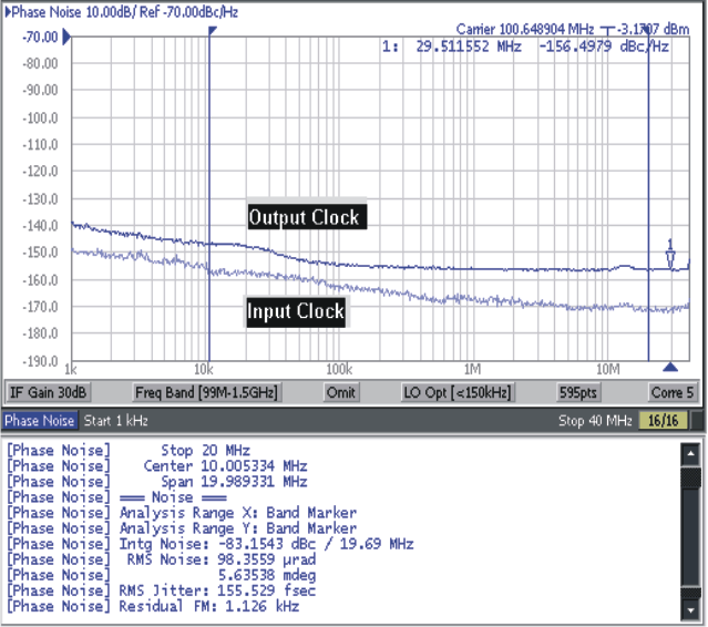
Input clock RMS jitter is 32 fs from 10 kHz to 20 MHz and additive RMS jitter is 152 fs, TA = 25°C, and VCC = 2.5 V
Figure 1. 100-MHz Input and Output Phase Noise Plot
