SCAS897A July 2010 – October 2016 CDCLVD1213
PRODUCTION DATA.
- 1 Features
- 2 Applications
- 3 Description
- 4 Revision History
- 5 Pin Configuration and Functions
- 6 Specifications
- 7 Parameter Measurement Information
- 8 Detailed Description
- 9 Application and Implementation
- 10Power Supply Recommendations
- 11Layout
- 12Device and Documentation Support
- 13Mechanical, Packaging, and Orderable Information
Package Options
Mechanical Data (Package|Pins)
- RGT|16
Thermal pad, mechanical data (Package|Pins)
- RGT|16
Orderable Information
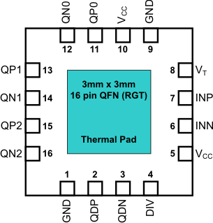
5 Pin Configuration and Functions
RGT Package
16-Pin VQFN
Top View

Pin Functions
| PIN | TYPE | DESCRIPTION | |
|---|---|---|---|
| NO. | NAME | ||
| 1, 9 | GND | Ground | Device ground |
| 2, 3 | QDP, QDN | Output | Differential divided LVDS output pair |
| 4 | DIV | Input with an internal 200-kΩ pullup and pulldown | Divider selection – selects divider ratio for QD output (see Table 1). |
| 5, 10 | VCC | Power | 2.5-V supply for the device |
| 6, 7 | INN, INP | Input | Differential input pair |
| 8 | VT | Input | Input for threshold voltage |
| 11, 12 | QP0, QN0 | Output | Differential LVDS output pair number 0 |
| 13, 14 | QP1, QN1 | Output | Differential LVDS output pair number 1 |
| 15, 16 | QP2, QN2 | Output | Differential LVDS output pair number 2 |
| — | Thermal Pad | — | See thermal management recommendations |