SCAS759C April 2004 – July 2017 CDCM1802
PRODUCTION DATA.
- 1 Features
- 2 Applications
- 3 Description
- 4 Revision History
- 5 Pin Configuration and Functions
-
6 Specifications
- 6.1 Absolute Maximum Ratings
- 6.2 ESD Ratings
- 6.3 Recommended Operating Conditions
- 6.4 Thermal Information
- 6.5 Electrical Characteristics
- 6.6 Switching Characteristics
- 6.7 Jitter Characteristics
- 6.8 Supply Current Electrical Characteristics
- 6.9 Control Input Characteristics
- 6.10 Timing Requirements
- 6.11 Bias Voltage VBB
- 6.12 Typical Characteristics
- 7 Parameter Measurement Information
- 8 Detailed Description
- 9 Application and Implementation
- 10Power Supply Recommendations
- 11Layout
- 12Device and Documentation Support
- 13Mechanical, Packaging, and Orderable Information
Package Options
Mechanical Data (Package|Pins)
- RGT|16
Thermal pad, mechanical data (Package|Pins)
- RGT|16
Orderable Information
9 Application and Implementation
NOTE
Information in the following applications sections is not part of the TI component specification, and TI does not warrant its accuracy or completeness. TI’s customers are responsible for determining suitability of components for their purposes. Customers should validate and test their design implementation to confirm system functionality.
9.1 Application Information
9.1.1 LVPECL Receiver Input Termination
The input of the CDCM1802 has high impedance and comes with a very large common mode voltage range. For optimized noise performance it is recommended to properly terminate the PCB trace (transmission line).
Additional termination techniques can be found in the following application notes: SCAA062 and SCAA059.
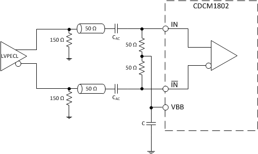 Figure 15. Recommended AC-Coupling LVPECL Receiver Input Termination
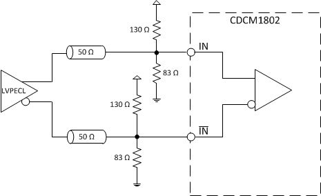 Figure 16. Recommended DC-Coupling LVPECL Receiver Input Termination
9.1.2 LVCMOS Receiver Input Termination
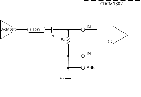
NOTE:
CAC − AC-coupling capacitor (for example, 10 nF)CCT − Capacitor keeps voltage at IN constant (for example, 10 nF)
Rdc − Load and correct duty cycle (for example, 50 Ω)
VBB − Bias voltage output
9.2 Typical Application
Figure 18 shows a fanout buffer application.
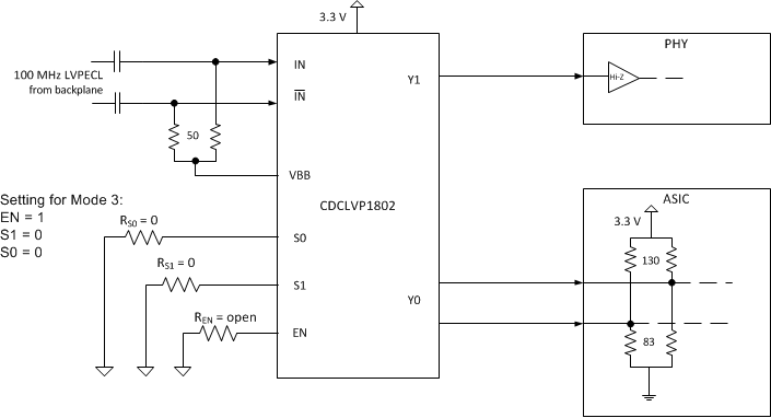 Figure 18. Typical Application Schematic, CDCM1802
9.2.1 Design Requirements
The CDCM1802 shown in Figure 18 is configured to be able to select an 100-MHz LVPECL clock from the backplane. The signal can be fanned out to desired devices, as shown. The CDCM1802 offers internal dividers for both the LVCMOS and LVPECL output. In the example the LVCMOS output is divided by 4 and the LVPECL output is divided by 1.
- The PHY device receive a single ended 25-MHz signal. Optionally a series resistance can be placed close to the output to match transmission line impedance and reduce reflections.
- The ASIC is capable of DC coupling with a 3.3-V LVPECL driver such as the CDCM1802. This ASIC features internal termination so no additional components are needed.
- S0, S1, EN needs to be set accordingly to ensure the required divider setting.
9.2.2 Detailed Design Procedure
Refer to LVPECL Receiver Input Termination for proper input terminations, dependent on single-ended or differential inputs.
Refer to Figure 9 and Figure 10 for output termination schemes depending on the receiver application.
Refer to Table 1 for setting the desired divider modes.
9.2.3 Application Curve
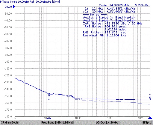
| Input (Vectron C5310A1) = 83 fs, rms | Output (LVPECL, divide 1) = 134 fs, rms | |||
| additive jitter = 105 fs, rms (typ) | ||||