SCAS759C April 2004 – July 2017 CDCM1802
PRODUCTION DATA.
- 1 Features
- 2 Applications
- 3 Description
- 4 Revision History
- 5 Pin Configuration and Functions
-
6 Specifications
- 6.1 Absolute Maximum Ratings
- 6.2 ESD Ratings
- 6.3 Recommended Operating Conditions
- 6.4 Thermal Information
- 6.5 Electrical Characteristics
- 6.6 Switching Characteristics
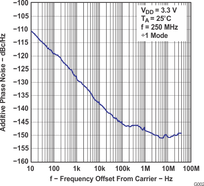
- 6.7 Jitter Characteristics
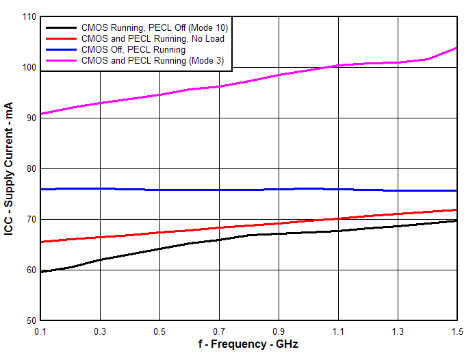
- 6.8 Supply Current Electrical Characteristics
- 6.9 Control Input Characteristics
- 6.10 Timing Requirements
- 6.11 Bias Voltage VBB
- 6.12 Typical Characteristics
- 7 Parameter Measurement Information
- 8 Detailed Description
- 9 Application and Implementation
- 10Power Supply Recommendations
- 11Layout
- 12Device and Documentation Support
- 13Mechanical, Packaging, and Orderable Information
Package Options
Mechanical Data (Package|Pins)
- RGT|16
Thermal pad, mechanical data (Package|Pins)
- RGT|16
Orderable Information
6 Specifications
6.1 Absolute Maximum Ratings
over operating free-air temperature range (unless otherwise noted) (1)| MIN | MAX | UNIT | ||
|---|---|---|---|---|
| VDD | Supply voltage | –0.3 | 3.8 | V |
| VI | Input voltage | –0.2 | (VDD + 0.2) | V |
| VO | Output voltage | –0.2 | (VDD + 0.2) | V |
| Yn, Yn, IOSD | Differential short circuit current | Continuous | ||
| TJ | Maximum junction temperature | 125 | 125 | °C |
| Tstg | Storage temperature | −65 | 150 | °C |
(1) Stresses beyond those listed under Absolute Maximum Ratings may cause permanent damage to the device. These are stress ratings only, which do not imply functional operation of the device at these or any other conditions beyond those indicated under Recommended Operating Conditions. Exposure to absolute-maximum-rated conditions for extended periods may affect device reliability.
6.2 ESD Ratings
| VALUE | UNIT | |||
|---|---|---|---|---|
| V(ESD) | Electrostatic discharge | Human-body model (HBM), per ANSI/ESDA/JEDEC JS-001(1) | ±3000 | V |
| Charged-device model (CDM), per JEDEC specification JESD22-C101(2) | ±1500 | |||
(1) JEDEC document JEP155 states that 500-V HBM allows safe manufacturing with a standard ESD control process.
(2) JEDEC document JEP157 states that 250-V CDM allows safe manufacturing with a standard ESD control process.
6.3 Recommended Operating Conditions
over operating free-air temperature range (unless otherwise noted)| MIN | NOM | MAX | UNIT | ||
|---|---|---|---|---|---|
| VDD | Supply voltage | 3 | 3.3 | 3.6 | V |
| VDD | Supply voltage (only functionality) | 2.375 | 3.6 | V | |
| TA | Operating free-air temperature | –40 | 85 | °C | |
6.4 Thermal Information
| THERMAL METRIC(1) | CDCM1802 | UNIT | |
|---|---|---|---|
| RGT (VQFN) | |||
| 16 PINS | |||
| RθJA | Junction-to-ambient thermal resistance | 48.4 | °C/W |
| RθJC(top) | Junction-to-case (top) thermal resistance | 66.9 | °C/W |
| RθJB | Junction-to-board thermal resistance | 22.5 | °C/W |
| ψJT | Junction-to-top characterization parameter | 1.7 | °C/W |
| ψJB | Junction-to-board characterization parameter | 22.5 | °C/W |
| RθJC(bot) | Junction-to-case (bottom) thermal resistance | 5.8 | °C/W |
(1) For more information about traditional and new thermal metrics, see the Semiconductor and IC Package Thermal Metrics application report.
6.5 Electrical Characteristics
over recommended operating free-air temperature range (unless otherwise noted)| PARAMETER | TEST CONDITIONS | MIN | TYP | MAX | UNIT | |
|---|---|---|---|---|---|---|
| LVPECL INPUT IN, IN | ||||||
| fclk | Input frequency | 0 | 800 | MHz | ||
| VCM | High-level input common mode | 1 | VDD − 0.3 | V | ||
| VIN | Input voltage swing between IN and IN | See (1) | 500 | 1300 | mV | |
| See (2) | 150 | 1300 | ||||
| IIN | Input current | VI = VDD or 0 V | ±10 | µA | ||
| RIN | Input impedance | 300 | kΩ | |||
| CI | Input capacitance at IN, IN | 1 | pF | |||
| LVPECL OUTPUT DRIVER Y0, Y0 | ||||||
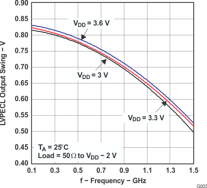
| fclk | Output frequency (see Figure 3) | 0 | 800 | MHz | ||
| VOH | High-level output voltage | Termination with 50 Ω to VDD − 2 V | VDD − 1.18 | VDD – 0.81 | V | |
| VOL | Low-level output voltage | Termination with 50 Ω to VDD − 2 V | VDD − 1.98 | VDD – 1.55 | V | |
| VO | Output voltage swing between Y and Y (see Figure 3) | Termination with 50 Ω to VDD − 2 V | 500 | mV | ||
| IOZL | Output 3-state | VDD = 3.6 V, VO = 0 V | 5 | µA | ||
| IOZH | VDD = 3.6 V, VO = VDD – 0.8 V | 10 | µA | |||
| CO | Output capacitance | VO = VDD or GND | 1 | pF | ||
| LOAD | Expected output load | 50 | Ω | |||
| LVCMOS OUTPUT PARAMETER, Y1 | ||||||
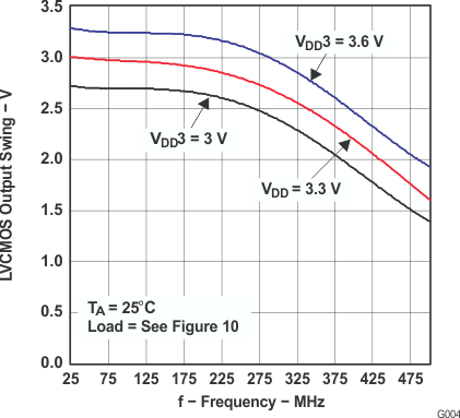
| fclk | Output frequency(4) (see Figure 4) | 0 | 200 | MHz | ||
| VOH | High-level output voltage | VDD = min to max, IOH = −100 µA | VDD – 0.1 | V | ||
| VDD = 3 V, IOH = −6 mA | 2.4 | |||||
| VDD = 3 V, IOH = −12 mA | 2 | |||||
| VOL | Low-level output voltage | VDD = min to max, IOL = 100 µA | 0.1 | V | ||
| VDD = 3 V, IOL = 6 mA | 0.5 | |||||
| VDD = 3 V, IOL = 12 mA | 0.8 | |||||
| IOH | High-level output current | VDD = 3.3 V, VO = 1.65 V | −29 | mA | ||
| IOL | Low-level output current | VDD = 3.3 V, VO = 1.65 V | 37 | mA | ||
| IOZ | High-impedance state output current | VDD = 3.6 V, VO = VDD or 0 V | ±5 | µA | ||
| CO | Output capacitance | VDD = 3.3 V | 2 | pF | ||
| Load | Expected output loading (see Figure 9) | 10 | pF | |||
(1) Required to maintain AC specifications
(2) Required to maintain device functionality
(3) For a 800-MHz signal, the 50-ps error would result into a duty cycle distortion of ±4% when driven by an ideal clock input signal.
(4) Operating the CDCM1802 LVCMOS output above the maximum frequency will not cause a malfunction to the device, but the Y1 output signal swing will not achieve enough signal swing to meet the output specification. Therefore, the CDCM1802 can be operated at higher frequencies, while the LVCMOS output Y1 becomes unusable.
(5) For a 200-MHz signal, the 150-ps error would result in a duty cycle distortion of ±3% when driven by an ideal clock input signal.
6.6 Switching Characteristics
over operating free-air temperature range (unless otherwise noted)| PARAMETER | TEST CONDITIONS | MIN | TYP | MAX | UNIT | |
|---|---|---|---|---|---|---|
| LVPECL OUTPUT DRIVER Y0, Y0 | ||||||
| tDuty | Output duty cycle distortion(3) | Crossing point-to-crossing point distortion | −50 | 50 | ps | |
| tsk(pp) | Part-to-part skew | Any Y0 (see Note A in Figure 7) | 50 | ps | ||
| tr/tf | Rise and fall time | 20% to 80% of VOUTPP
(see Figure 8) |
200 | 350 | ps | |
| LVPECL INPUT-TO-LVPECL OUTPUT PARAMETER | ||||||
| tpd(lh) | Propagation delay rising edge | VOX to VOX | 320 | 600 | ps | |
| tpd(hl) | Propagation delay falling edge | VOX to VOX | 320 | 600 | ps | |
| tsk(p) | LVPECL pulse skew (see Note B in Figure 7) |
VOX to VOX | 100 | ps | ||
| LVCMOS OUTPUT PARAMETER, Y1 | ||||||
| tskLVCMOS(o) | Output skew between the LVCMOS output Y1 and LVPECL output Y0 | VOX to VDD / 2 (see Figure 7) | 1.6 | ns | ||
| tDuty | Output duty cycle distortion(5) | Measured at VDD / 2 | −150 | 150 | ps | |
| tsk(pp) | Part-to-part skew | Y1 (see Note A in Figure 7) | 300 | ps | ||
| tpd(lh) | Propagation delay rising edge from IN to Y1 | VOX to VDD / 2 load (see Figure 9) | 1.6 | 2.6 | ns | |
| tpd(hl) | Propagation delay falling edge from IN to Y1 | VOX to VDD / 2 load (see Figure 9) | 1.6 | 2.6 | ns | |
| tr | Output rise slew rate | 20% to 80% of swing (see Figure 9) |
1.4 | 2.3 | V/ns | |
| tf | Output fall slew rate | 80% to 20% of swing (see Figure 9) |
1.4 | 2.3 | V/ns | |
6.7 Jitter Characteristics
over operating free-air temperature range (unless otherwise noted)| PARAMETER | TEST CONDITIONS | MIN | TYP | MAX | UNIT | |
|---|---|---|---|---|---|---|
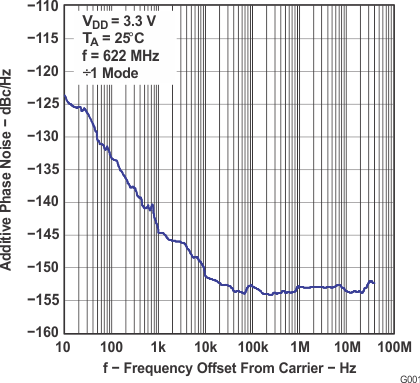
| tjitterLVPECL | Additive phase jitter from input to LVPECL output Y0 (see Figure 1) |
12 kHz to 20 MHz, fout = 250 MHz to 800 MHz, divide by 1 mode | 0.15 | ps rms | ||
| 50 kHz to 40 MHz, fout = 250 MHz to 800 MHz, divide by 1 mode | 0.25 | ps rms | ||||
| tjitterLVCMOS | Additive phase jitter from input to LVCMOS output Y1 (see Figure 2) |
12 kHz to 20 MHz, fout = 250 MHz, divide by 1 mode | 0.25 | ps rms | ||
| 50 kHz to 40 MHz, fout = 250 MHz, divide by 1 mode | 0.4 | ps rms | ||||
6.8 Supply Current Electrical Characteristics
over recommended operating free-air temperature range (unless otherwise noted)| PARAMETER | TEST CONDITIONS | MIN | TYP | MAX | UNIT | ||
|---|---|---|---|---|---|---|---|
| IDD | Supply current | Full load | All outputs enabled and terminated with 50 Ω to VDD − 2 V on LVPECL outputs and 10 pF on LVCMOS output, f = 800 MHz for LVPECL outputs and 200 MHz for LVCMOS, VDD = 3.3 V |
100 | mA | ||
| No load | Outputs enabled, no output load, f = 800 MHz for LVPECL outputs and 200 MHz for LVCMOS, VDD = 3.6 V | 85 | mA | ||||
| IDDZ | Supply current, 3-state | All outputs 3-state by control logic, f = 0 Hz, VDD = 3.6 V | 0.5 | mA | |||
6.9 Control Input Characteristics
over operating free-air temperature range (unless otherwise noted)| PARAMETER | TEST CONDITIONS | MIN | TYP | MAX | UNIT | |
|---|---|---|---|---|---|---|
| Rpullup | Internal pullup resistor on S0, S1, and EN input | 42 | 60 | 78 | kΩ | |
| VIH(H) | Three level input high, S0, S1, and EN pin(1) | 0.9 × VDD | V | |||
| VIM(M) | Three level input MID, S0, S1, and EN pin | 0.3 × VDD | 0.7 × VDD | V | ||
| VIL(L) | Three level low, S0, S1, and EN pin | 0.1 × VDD | V | |||
| IIH | Input current, S0, S1, and EN pin | VI = VDD | –5 | µA | ||
| IIL | Input current, S0, S1, and EN pin | VI = GND | 38 | 85 | µA | |
(1) Leaving this pin floating automatically pulse the logic level high to VDD through an internal pullup resistor of 60 kΩ.
6.10 Timing Requirements
| MIN | NOM | MAX | UNIT | ||
|---|---|---|---|---|---|
| tsu | Setup time, S0, S1, and EN pin before clock IN | 25 | ns | ||
| th | Hold time, S0, S1, and EN pin after clock IN | 0 | ns | ||
| t(disable) | Time between latching the EN low transition and when all outputs are disabled (how much time is required until the outputs turn off) | 10 | ns | ||
| t(enable) | Time between latching the EN low-to-high transition and when outputs are enabled based on control settings (how much time passes before the outputs carry valid signals) | 1 | μs | ||
6.11 Bias Voltage VBB
over operating free-air temperature range (unless otherwise noted)| PARAMETER | TEST CONDITIONS | MIN | TYP | MAX | UNIT | |
|---|---|---|---|---|---|---|
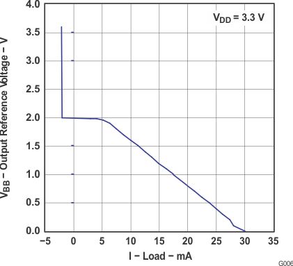
| VBB | Output reference voltage | VDD = 3 V–3.6 V, IBB = –0.2 mA | VDD – 1.4 | VDD – 1.2 | V | |
6.12 Typical Characteristics
Frequency Offset From Carrier − LVPECL
Frequency Offset From Carrier − LVCMOS
