SNAS682 March 2016 CDCM6208V2G
PRODUCTION DATA.
- 1 Features
- 2 Applications
- 3 Description
- 4 Simplified Schematics
- 5 Revision History
- 6 Description (continued)
- 7 Pin Configuration and Functions
-
8 Specifications
- 8.1 Absolute Maximum Ratings
- 8.2 ESD Ratings
- 8.3 Recommended Operating Conditions
- 8.4 Thermal Information, Airflow = 0 LFM
- 8.5 Thermal Information, Airflow = 150 LFM
- 8.6 Thermal Information, Airflow = 250 LFM
- 8.7 Thermal Information, Airflow = 500 LFM
- 8.8 Single Ended Input Characteristics
- 8.9 Single Ended Input Characteristics (PRI_REF, SEC_REF)
- 8.10 Differential Input Characteristics (PRI_REF, SEC_REF)
- 8.11 Crystal Input Characteristics (SEC_REF)
- 8.12 Single Ended Output Characteristics (STATUS1, STATUS0, SDO, SDA)
- 8.13 PLL Characteristics
- 8.14 LVCMOS Output Characteristics
- 8.15 LVPECL (High-Swing CML) Output Characteristics
- 8.16 CML Output Characteristics
- 8.17 LVDS (Low-Power CML) Output Characteristics
- 8.18 HCSL Output Characteristics
- 8.19 Output Skew and Sync to Output Propagation Delay Characteristics
- 8.20 Device Individual Block Current Consumption
- 8.21 Worst Case Current Consumption
- 8.22 I2C TIMING
- 8.23 SPI Timing Requirements
- 8.24 Typical Characteristics
- 9 Parameter Measurement Information
- 10Detailed Description
-
11Application and Implementation
- 11.1 Application Information
- 11.2
Typical Applications
- 11.2.1
Design Requirements
- 11.2.1.1 Device Block-level Description
- 11.2.1.2 Device Configuration Control
- 11.2.1.3 Configuring the RESETN Pin
- 11.2.1.4 Preventing False Output Frequencies in SPI/I2C Mode at Startup:
- 11.2.1.5 Power Down
- 11.2.1.6 Device Power Up Timing:
- 11.2.1.7 Input Mux and Smart Input Mux
- 11.2.1.8 Universal INPUT Buffer (PRI_REF, SEC_REF)
- 11.2.1.9 VCO Calibration
- 11.2.1.10 Reference Divider (R)
- 11.2.1.11 Input Divider (M)
- 11.2.1.12 Feedback Divider (N)
- 11.2.1.13 Prescaler Dividers (PS_A, PS_B)
- 11.2.1.14 Phase Frequency Detector (PFD)
- 11.2.1.15 Charge Pump (CP)
- 11.2.1.16
Programmable Loop Filter
- 11.2.1.16.1 Loop Filter Component Selection
- 11.2.1.16.2 Device Output Signaling
- 11.2.1.16.3 Integer Output Divider (IO)
- 11.2.1.16.4 Fractional Output Divider (FOD)
- 11.2.1.16.5 Output Synchronization
- 11.2.1.16.6 Output MUX on Y4 and Y5
- 11.2.1.16.7 Staggered CLK Output Powerup for Power Sequencing of a DSP
- 11.2.2 Detailed Design Procedure
- 11.2.3 Application Performance Plots
- 11.2.1
Design Requirements
- 12Power Supply Recommendations
- 13Layout
- 14Device and Documentation Support
- 15Mechanical, Packaging, and Orderable Information
Package Options
Mechanical Data (Package|Pins)
- RGZ|48
Thermal pad, mechanical data (Package|Pins)
- RGZ|48
Orderable Information
9 Parameter Measurement Information
9.1 Characterization Test Setup
This section describes the characterization test setup of each block in the CDCM6208V2G.
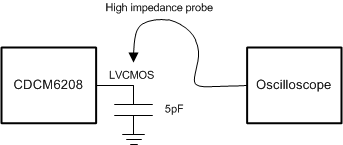 Figure 8. LVCMOS Output AC Configuration During Device Test (VOH, VOL, tSLEW)
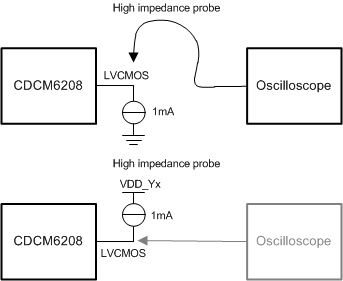 Figure 9. LVCMOS Output DC Configuration During Device Test
 Figure 10. LVCMOS Output AC Configuration During Device Phase Noise Test
 Figure 11. LVDS, CML, and LVPECL Output AC Configuration During Device Test
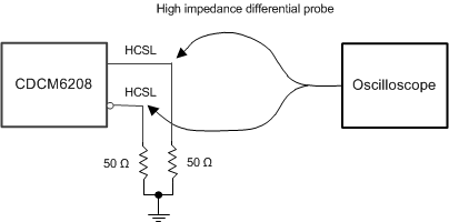 Figure 12. HCSL Output DC Configuration During Device Test
 Figure 13. HCSL Output AC Configuration During Device Test
 Figure 14. LVCMOS Input DC Configuration During Device Test
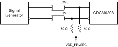 Figure 15. CML Input DC Configuration During Device Test
 Figure 16. LVDS Input DC Configuration During Device Test
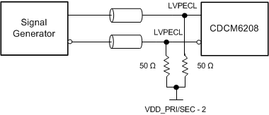 Figure 17. LVPECL Input DC Configuration During Device Test
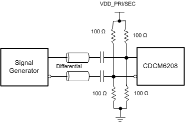 Figure 18. Differential Input AC Configuration During Device Test
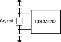 Figure 19. Crystal Reference Input Configuration During Device Test
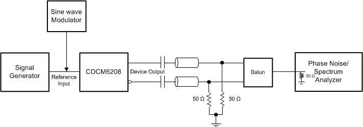 Figure 20. Jitter transfer Test Setup
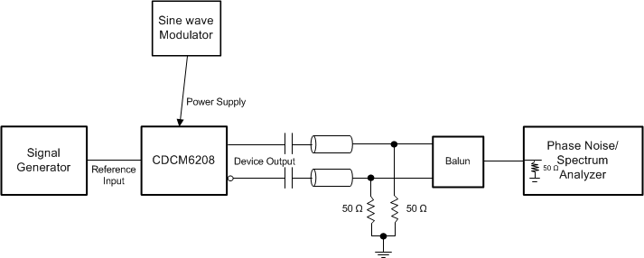 Figure 21. PSNR Test Setup
 Figure 22. Differential Output Voltage and Rise and Fall Time
 Figure 23. Single Ended Output Voltage and Rise and Fall Time
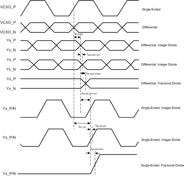 Figure 24. Differential and Single Ended Output Skew and Propagation Delay